
产品应用与封装尺寸
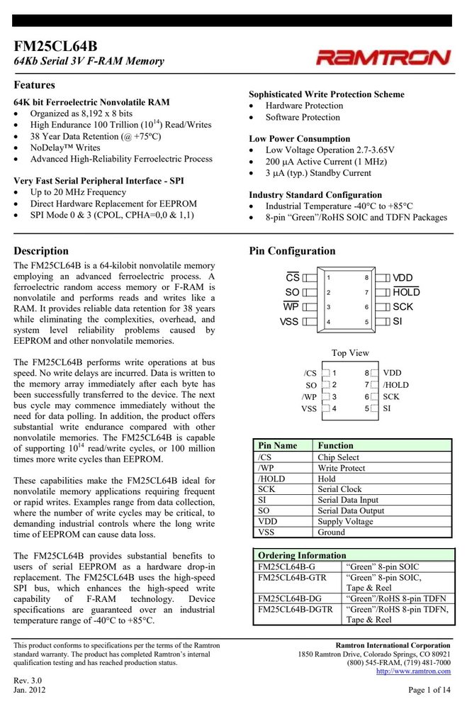
图纸取自原厂规格书,点击可放大查看原始尺寸标注。
引脚定义与内部结构
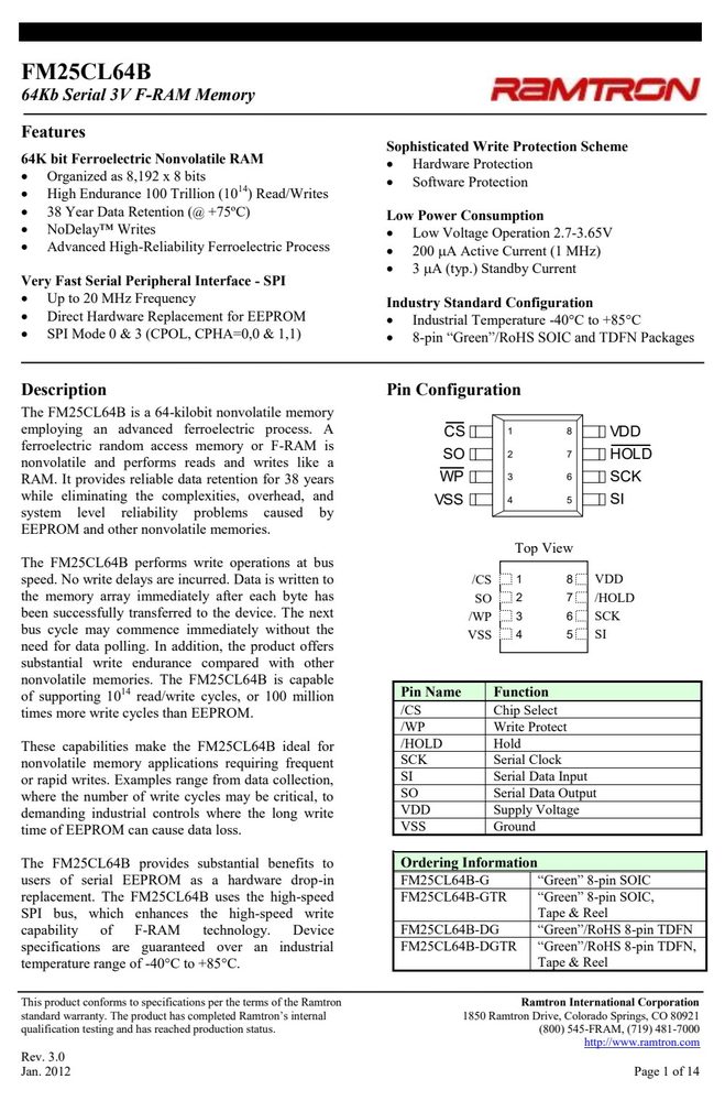
| 引脚 | 符号 | 名称 |
|---|---|---|
| 5 | S | |
| 6 | S | |
| 7 | H | |
| 8 | V |
数据来源:原厂规格书引脚图
产品特点 Features
- Sophisticated Write Protection Scheme code, the FM25CL64B will return one byte with the contents of the Status Register. The Status Register is described in detail in a later section.
- Figure 7. RDSR
- Figure 8. WRSR Bus
- Status Register & Write Protection to the Status Register, not the memory array. Prior to sending the WRSR command, the user must send a
- WREN command to enable writes. Note that executing a WRSR command is a write operation and therefore clears the Write Enable Latch.
- Configuration
- (WREN not shown) yellow). The WEL flag indicates the state of the
- Table 2. Status Register
- Bit 7 6 5 4 3 2 1 0
- Name WPEN 0 0 0 BP1 BP0 WEL 0
- Bits 0 and 4-6 are fixed at 0 and cannot be modified.
- Note that bit 0 (“Ready” in EEPROMs) is unnecessary as the F-RAM writes in real-time and is never busy. The WPEN, BP1 and BP0 control write state. This bit is internally set and cleared via the
- WREN and WRDI commands, respectively.
- BP1 and BP0 are memory block write protection bits.
- They specify portions of memory that are write- protected as shown in the following table.
- Table 3. Block Memory Write Protection
绝对最大额定值 Absolute Maximum Ratings(TA = 25°C)
超过下表数值可能造成器件永久损坏,设计时请留余量。
| 符号 | 参数 | 最小 | 最大 | 单位 | 备注 |
|---|---|---|---|---|---|
| FM25CL64B | - 64Kb 3V | SPI F-RAM | |||
| f | SCK Clock Frequency | 0 | 20 | MHz | |
| t | Clock High Time | 22 | ns | 1 | |
| t | Clock Low Time | 22 | ns | 1 | |
| t | Chip Select Setup | 10 | ns | ||
| t | Chip Select Hold | 10 | ns | ||
| t | Output Disable Time | 20 | ns | 2 | |
| t | Output Data Valid Time | 20 | ns | ||
| t | Output Hold Time | 0 | ns | ||
| t | Deselect Time | 60 | ns | ||
| t | Data In Rise Time | 50 | ns | 2,3 | |
| t | Data In Fall Time | 50 | ns | 2,3 | |
| t | Data Setup Time | 5 | ns | ||
| t | Data Hold Time | 5 | ns | ||
| t | /HOLD Setup Time | 10 | ns | ||
| t | /HOLD Hold Time | 10 | ns | ||
| t | /HOLD Low to Hi-Z | 20 | ns | 2 | |
| t | /HOLD High to Data Active | 20 | ns | 2 | |
| Capacitance | (T = 25 C, f=1.0 MHz, V = | 3.3V) | |||
| C | Output Capacitance (SO) | - | 8 | pF | 1 |
| C | Input Capacitance | - | 6 | pF | 1 |
数据来源:原厂规格书
电气特性 Electrical Characteristics(TA = 25°C)
| 符号 | 参数 | 最小 | 最大 | 单位 | 备注 |
|---|---|---|---|---|---|
| FM25CL64B | - 64Kb 3V | SPI F-RAM | |||
| f | SCK Clock Frequency | 0 | 20 | MHz | |
| t | Clock High Time | 22 | ns | 1 | |
| t | Clock Low Time | 22 | ns | 1 | |
| t | Chip Select Setup | 10 | ns | ||
| t | Chip Select Hold | 10 | ns | ||
| t | Output Disable Time | 20 | ns | 2 | |
| t | Output Data Valid Time | 20 | ns | ||
| t | Output Hold Time | 0 | ns | ||
| t | Deselect Time | 60 | ns | ||
| t | Data In Rise Time | 50 | ns | 2,3 | |
| t | Data In Fall Time | 50 | ns | 2,3 | |
| t | Data Setup Time | 5 | ns | ||
| t | Data Hold Time | 5 | ns | ||
| t | /HOLD Setup Time | 10 | ns | ||
| t | /HOLD Hold Time | 10 | ns | ||
| t | /HOLD Low to Hi-Z | 20 | ns | 2 | |
| t | /HOLD High to Data Active | 20 | ns | 2 | |
| Capacitance | (T = 25 C, f=1.0 MHz, V = | 3.3V) | |||
| C | Output Capacitance (SO) | - | 8 | pF | 1 |
| C | Input Capacitance | - | 6 | pF | 1 |
订货信息与供货形式
| 包装 | & | 包装2 |
|---|---|---|
| Tape | & | Reel |
| FM25CL64B-DG | “Green”/RoHS | 8-pin TDFN |
| FM25CL64B-DGTR | “Green”/RoHS | 8-pin TDFN, |
| Tape | & | Reel |
| Ramtron | International Corporation |