
引脚定义与内部结构
| 引脚 | 符号 | 名称 |
|---|---|---|
| 7 | E N | |
| 6 | F B | |
| 5 | N C | |
| 4 | G ND | |
| 3 | B OOT | |
| 2 | V IN | |
| 1 | SW |
数据来源:原厂规格书引脚图
关键参数速览
- 工作温度 TA
- tested at 25°C. Limits
产品特点 Features
- The LM22676 switching regulator provides all of the
- Wide Input Voltage Range: 4.5 V to 42 V
- 1 functions necessary to implement an efficient high
- Internally Compensated Voltage Mode Control voltage step-down (buck) regulator using a minimum
- Stable with Low ESR Ceramic Capacitors of external components. This easy to use regulator
- 120 mΩ N-Channel MOSFET PFM Package incorporates a 42 V N-channel MOSFET switch capable of providing up to 3 A of load current.
- 100 mΩ N-Channel MOSFET PSOP-8 Package
- Excellent line and load regulation along with high
- Output Voltage Options:
- -ADJ (Outputs as Low as 1.285 V) offers short minimum on-time, allowing the widest
- -5.0 (Output Fixed to 5 V) ratio between input and output voltages. Internal loop
- ±1.5% Feedback Reference Accuracy compensation means that the user is free from the tedious task of calculating the loop compensation
- Switching Frequency of 500 kHz components. Fixed 5 V output and adjustable output
- –40°C to 125°C Operating Junction voltage options are available. A switching frequency
- Temperature Range of 500 kHz allows for small external components and
- Precision Enable Pin good transient response. A precision enable input allows simplification of regulator control and system
绝对最大额定值 Absolute Maximum Ratings(TA = 25°C)
超过下表数值可能造成器件永久损坏,设计时请留余量。
| 1 | 特性 | 12 | 7.4 | 器件 | Functional | Modes........................................ | 10 |
|---|---|---|---|---|---|---|---|
| 10.2 | Layout | Examples................................................... | 18 | ||||
| 10.3 | Thermal | Considerations........................................ | 19 |
数据来源:原厂规格书
电气特性 Electrical Characteristics(TA = 25°C)
| 参数 | 测试条件 | MIN(1) | TYP(2) | MAX(1) | 单位 |
|---|---|---|---|---|---|
| V = 8 V to 42 V | 4.925 | 5.0 | 5.075 | ||
| V = 8 V to 42 V, –40°C ≤ T ≤ 125°C | 4.9 | 5.1 | |||
| V = 4.7 V to 42 V | 1.266 | 1.285 | 1.304 | ||
| V = 4.7 V to 42 V, –40°C ≤ T ≤ 125°C V = 5 V | 1.259 | 3.4 | 1.311 | ||
| I Quiescent Current | mA | ||||
| V = 5 V, –40°C ≤ T ≤ 125°C | 6 | ||||
| I Standby Quiescent Current | EN Pin = 0 V | 25 | 40 | µA | |
| –40°C ≤ T ≤ 125°C | 3.35 | 5.5 | |||
| V = 42 V, EN Pin = 0 V, V = 0 V | 0.2 | 2 | µA | ||
| V = –1 V | 0.1 | 3 | µA | ||
| PFM Package | 0.12 | 0.16 | |||
| PFM Package | 0.22 | ||||
| SO PowerPAD Package | 0.10 | 0.16 | |||
| SO PowerPAD Package | 0.20 | ||||
| f Oscillator Frequency | kHz | ||||
| –40°C ≤ T ≤ 125°C | 400 | 600 | |||
| T Minimum Off-time | ns | ||||
| –40°C ≤ T ≤ 125°C | 100 | 300 | |||
| T Minimum On-time | 100 | ns | |||
| I Feedback Bias Current | V = 1.3 V (ADJ Version Only) Falling | 230 1.6 | nA | ||
| Falling, –40°C ≤ T ≤ 125°C | 1.3 | 1.9 | |||
| V Enable Voltage Hysteresis | 0.6 | V | |||
| I Enable Input Current | EN Input = 0 V | 6 | µA | ||
| T Thermal Shutdown Threshold | 150 | °C | |||
| Product Folder Links: LM22676 | LM22676-Q1 |
应用领域 Applications
产品应用与封装尺寸
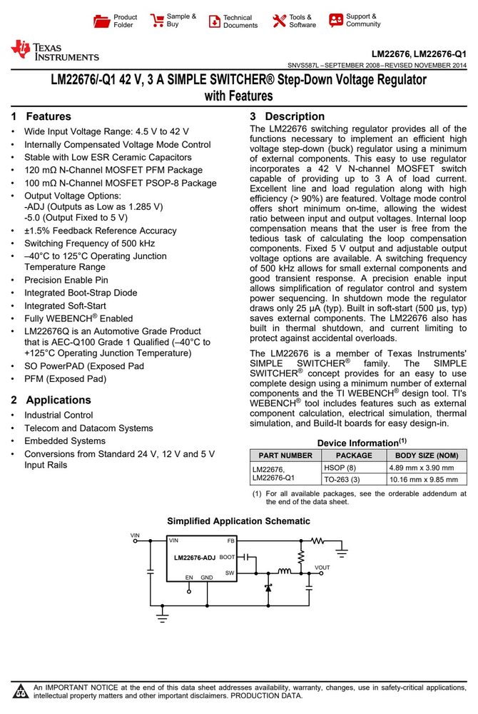
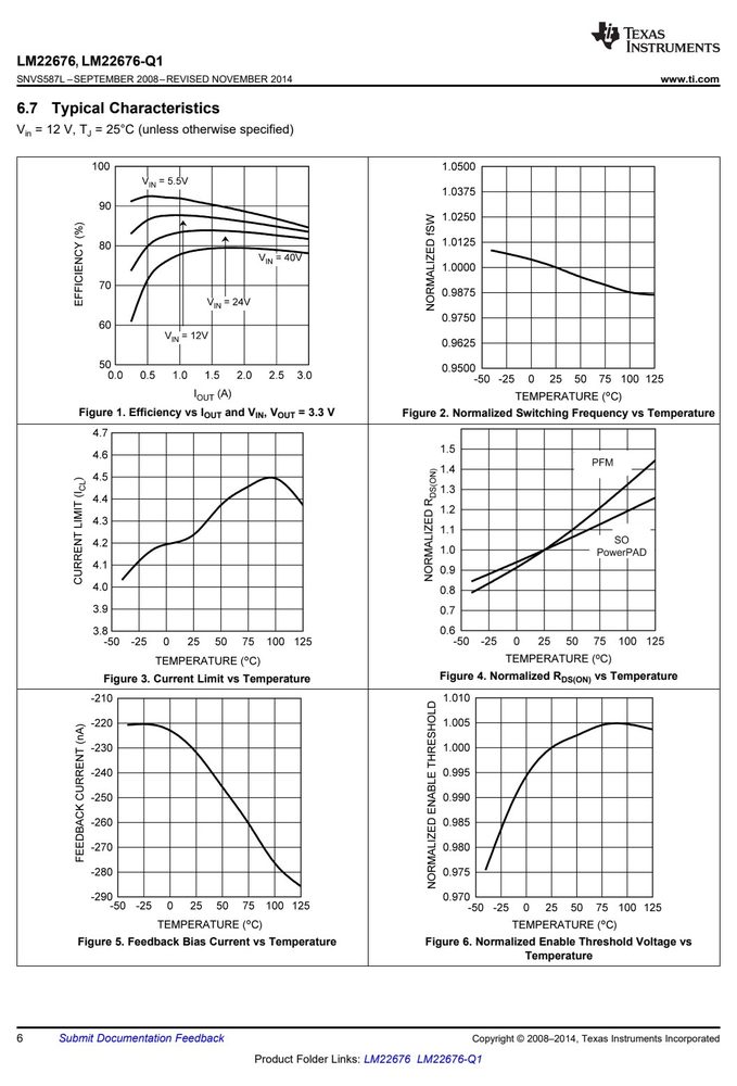
图纸取自该型号原厂规格书的应用电路与封装尺寸章节,点击图片可放大查看原始尺寸标注。