产品应用与封装尺寸
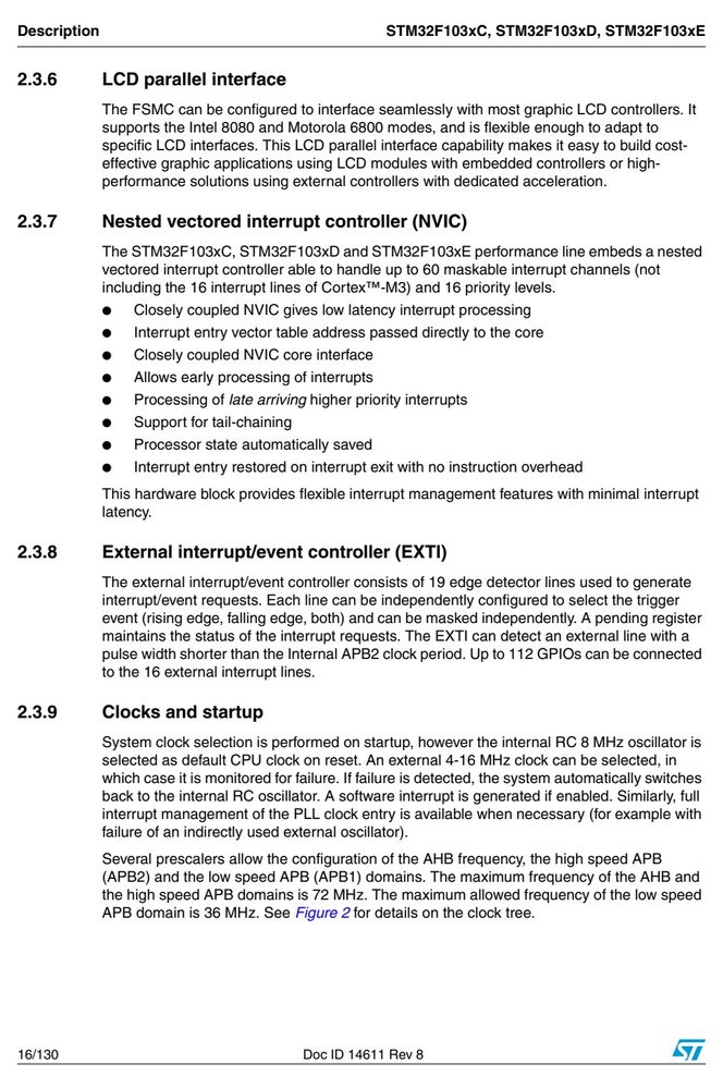
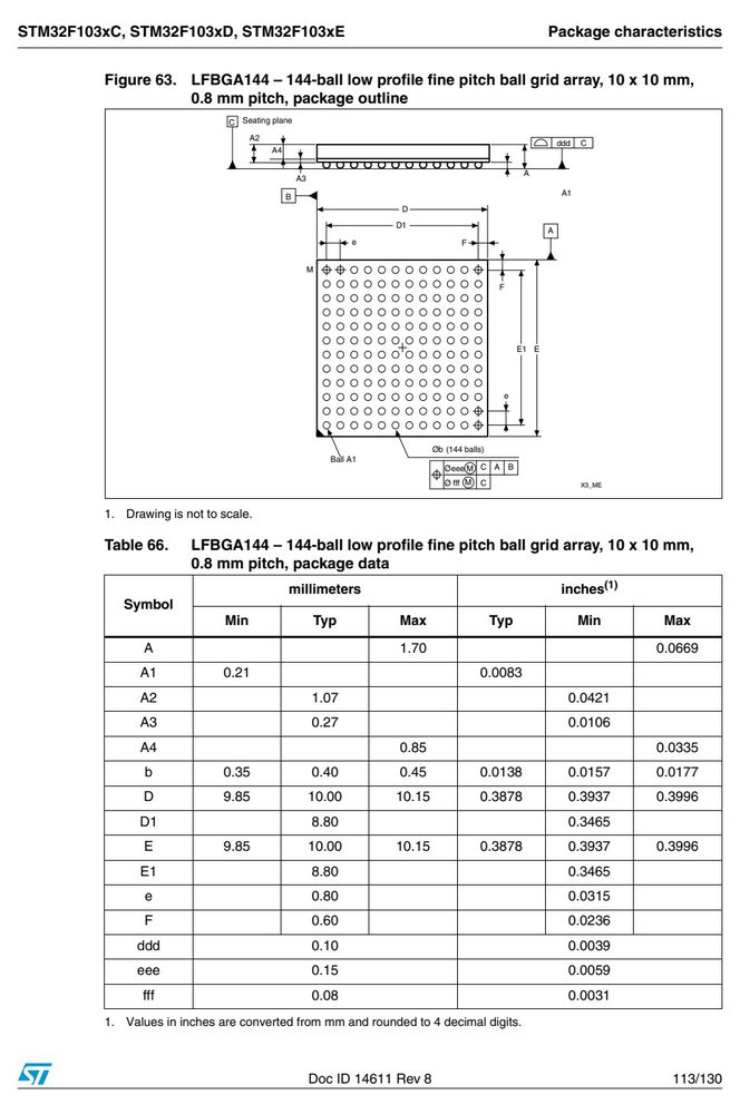
图纸取自原厂规格书,点击可放大查看原始尺寸标注。
引脚定义与内部结构
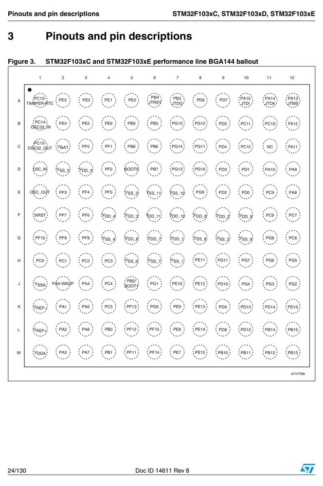
| 引脚 | 符号 | 名称 |
|---|---|---|
| 73 | NC | |
| 72 | PA 13 | |
| 71 | PA 12 | |
| 70 | PA 11 | |
| 69 | PA 10 | |
| 68 | PA 9 | |
| 67 | PA 8 | |
| 1 | I = input, O = output, S = supply. | |
| 3 | Function availability depends on the chosen device. |
数据来源:原厂规格书引脚图
产品特点 Features
- Core: ARM 32-bit Cortex™-M3 CPU
- 72 MHz maximum frequency,
- 1.25 DMIPS/MHz (Dhrystone 2.1) performance at 0 wait state memory access
- Single-cycle multiplication and hardware division
- Memories
- 256 to 512 Kbytes of Flash memory up to 64 Kbytes of SRAM
- Flexible static memory controller with 4
- Chip Select. Supports Compact Flash,
- SRAM, PSRAM, NOR and NAND memories
- LCD parallel interface, 8080/6800 modes
- Clock, reset and supply management
- 2.0 to 3.6 V application supply and I/Os
- POR, PDR, and programmable voltage detector (PVD)
- 4-to-16 MHz crystal oscillator
- Internal 8 MHz factory-trimmed RC
- Internal 40 kHz RC with calibration
绝对最大额定值 Absolute Maximum Ratings(TA = 25°C)
超过下表数值可能造成器件永久损坏,设计时请留余量。
| 符号 | 额定值 | 最小 | 最大 | 单位 |
|---|---|---|---|---|
| Stresses above the | absolute maximum ratings listed | in Table 7: Voltage | characteristics, | |
| at these conditions is | not implied. Exposure to | maximum rating conditions | for extended |
数据来源:原厂规格书
电气特性 Electrical Characteristics(TA = 25°C)
| 5.1 | 参数 | 条件 |
|---|---|---|
| Unless otherwise | specified, all voltages are referenced to V . | |
| Unless otherwise | specified the minimum and maximum values are guaranteed in the worst | |
| 100% of the | devices with an ambient temperature at T = 25 °C and T = T max (given by | |
| the selected | temperature range). | |
| are indicated in | the table footnotes and are not tested in production. Based on | |
| characterization, | the minimum and maximum values refer to sample tests and represent the | |
| mean value plus | or minus three times the standard deviation (mean±3Σ). | |
| Unless otherwise | specified, typical data are based on T = 25 °C, V = 3.3 V (for the | |
| 2 V ≤ V ≤ 3.6 | V voltage range). They are given only as design guidelines and are not | |
| Typical ADC | accuracy values are determined by characterization of a batch of samples from | |
| error less than | or equal to the value indicated (mean±2Σ). | |
| ● | All I/O pins are in input mode with a static value at V | or V (no load). |
| ● | The Flash access time is adjusted to f | frequency (0 wait state from 0 to 24 MHz, 1 |
| ● | Ambient temperature and V | supply voltage conditions summarized in Table 10. |
| 72 MHz | 51 | 30.5 |
| 48 MHz | 34.6 | 20.7 |
| 36 MHz | 26.6 | 16.2 |
| 24 MHz | 18.5 | 11.4 |
| 16 MHz | 12.8 | 8.2 |
| 4 MHz | 4.2 | 3.1 |
| 2 MHz | 2.7 | 2.1 |
| 1 MHz | 2 | 1.7 |
| 500 kHz | 1.6 | 1.4 |
| 125 kHz | 1.3 | 1.2 |
| 64 MHz | 45 | 27 |
| 48 MHz | 34 | 20.1 |
| 36 MHz | 26 | 15.6 |
| 24 MHz | 17.9 | 10.8 |
| 2 MHz | 2.1 | 1.5 |
| 1 MHz | 1.4 | 1.1 |
| 500 kHz | 1 | 0.8 |
| 125 kHz | 0.7 | 0.6 |
| The parameters | given in Table 28 are derived from tests | performed under ambient |
| temperature and V | supply voltage conditions summarized | in Table 10. |
| T able 28. PLL | characteristics | |
| PLL | input clock(2) 1 | 8.0 25 MHz |
| PLL | input clock duty cycle 40 | 60 % |
| f PLL | multiplier output clock 16 | 72 MHz |
| t PLL | lock time | 200 µs |
| Jitter | Cycle-to-cycle jitter | 300 ps |
| the range defined by | f . | |
| The characteristics | are given at T = –40 to 105 °C unless | otherwise specified. |
| T able 29. Flash | memory characteristics | |
| t 16-bit | programming time T = –40 to +105 °C | 40 52.5 70 µs |
| t Page (2 | KB) erase time T = –40 to +105 °C | 20 40 ms |
| t Mass erase | time T = –40 to +105 °C | 20 40 ms |
| f = 72 MHz with 2 wait | 28 mA | |
| states, V = 3.3 V | 7 mA | |
| f = 72 MHz, V = 3.3 | V | |
| I Supply | current HCLK DD | 5 mA |
| f = 72 MHz, V = 3.3 | V 50 µA | |
| V = 3.0 to 3.6 V | ||
| V Programming | voltage | 2 3.6 V |
| t | t | t |
| v(NWE_NE) | w(NWE) | h(NE_NWE) |
| t | t | t |
| v(A_NE) | v(Data_NADV) | h(Data_NWE) |
| FSMC_AD[15:0] | Address | Data |
| w(NE) | HCLK | HCLK |
| v(NWE_NE) | HCLK | HCLK |
| w(NWE) | HCLK | HCLK |
| w(NADV) | HCLK | HCLK |
订货信息与供货形式
| This | datasheet | provides | the | ordering | information | and | mechanical | 器件 | 特性 | of |
|---|---|---|---|---|---|---|---|---|---|---|
| the | STM32F103xC, | STM32F103xD | and | STM32F103xE | high-density | performance line | ||||
| please | refer to | Section | 2.2: | Full | compatibility | throughout | the family. | |||
| The | high-density | STM32F103xx | datasheet | should | be | read in | conjunction | with the | ||
| For | information | on | programming, | erasing | and | protection | of the | internal Flash | memory | |
| please | refer to | the | STM32F10xxx | Flash | programming | manual. | ||||
| The | reference | and Flash | programming | manuals | are both | available | from the |
应用领域 Applications
获取报价 / 申请样品
常备现货、免费送样、支持小批量试产。报出用量与封装要求,当天给报价与交期。
销售直线(点击可直接拨打)📞0755-82811939点击拨打📞0755-82812373点击拨打📞0755-82811915点击拨打📞0755-82811193点击拨打企业 QQ(点击跳转对话)💬QQ 2850611261企业QQ 对接💬QQ 2355817597企业QQ 对接💬QQ 3002728093企业QQ 对接💬QQ 2355817598企业QQ 对接
手机端点号码直接拨号/唤起 QQ;电脑端点座机会唤起系统拨号应用,点 QQ 会打开企业QQ 对话窗口。