
产品应用与封装尺寸
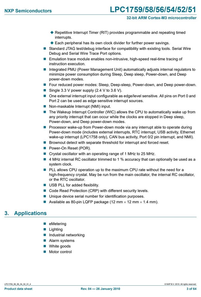
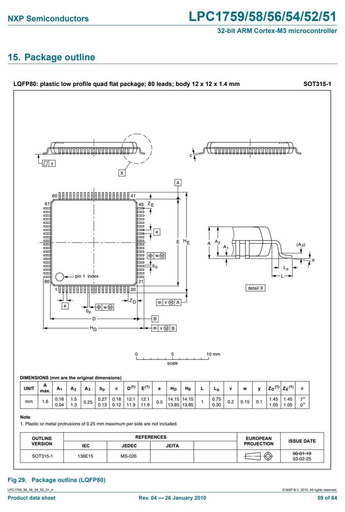
图纸取自原厂规格书,点击可放大查看原始尺寸标注。
关键参数速览
- 电源电压 VCC
- 3.6
产品特点 Features
- ARM Cortex-M3 processor, running at frequencies of up to 100 MHz
- (LPC1758/56/57/54/52/51) or of up to 120 MHz (LPC1759). A Memory Protection Unit
- (MPU) supporting eight regions is included.
- ARM Cortex-M3 built-in Nested Vectored Interrupt Controller (NVIC).
- Up to 512 kB on-chip flash programming memory. Enhanced flash memory accelerator enables high-speed 120 MHz operation with zero wait states.
- In-System Programming (ISP) and In-Application Programming (IAP) via on-chip bootloader software.
- On-chip SRAM includes:
- Up to 32 kB of SRAM on the CPU with local code/data bus for high-performance
- CPU access.
- Two/one 16 kB SRAM blocks with separate access paths for higher throughput.
- These SRAM blocks may be used for Ethernet (LPC1758 only), USB, and DMA memory, as well as for general purpose CPU instruction and data storage.
- Eight channel General Purpose DMA controller (GPDMA) on the AHB multilayer matrix that can be used with the SSP, I2S-bus, UART, the Analog-to-Digital and
- Digital-to-Analog converter peripherals, timer match signals, and for memory-to-memory transfers.
- Controls system exceptions and peripheral interrupts
- In the LPC1759/58/56/54/52/51, the NVIC supports 33 vectored interrupts
- 32 programmable interrupt priority levels, with hardware priority level masking
绝对最大额定值 Absolute Maximum Ratings(TA = 25°C)
超过下表数值可能造成器件永久损坏,设计时请留余量。
| 符号 | 参数 | 条件 | 最小 | 最大 | 单位 |
|---|---|---|---|---|---|
| V | regulator supply voltage | (3.3 V) | 2.4 | 3.6 | V |
| V | analog 3.3 V pad supply | voltage | −0.5 | +4.6 | V |
| V | input voltage on pin VREFP | −0.5 | +4.6 | V | |
| V | analog input voltage | on ADC related | −0.5 | +5.1 | V |
| V | input voltage | 5 V tolerant I/O DD(3V3) | [2] −0.5 | +5.5 | V |
| other I/O pins | [2][3] −0.5 | V DD(3V3) | + V | ||
| I | supply current | per supply pin | [4] - | 100 | mA |
| I | ground current | per ground pin | [4] - | 100 | mA |
| I | I/O latch-up current | −(0.5V ) < V | - | 100 | mA |
| latch | DD(3V3) I < (1.5V ); DD(3V3) T < 125 °C | ||||
| T | storage temperature | [5] −65 | +150 | °C | |
| P | total power dissipation (per | package) based on package | - | 1.5 | W |
| V | electrostatic discharge | voltage human body | [6] −4 000 | +4 000 | V |
数据来源:原厂规格书
电气特性 Electrical Characteristics(TA = 25°C)
| 符号 | 参数 | 条件 | 最小 | 典型 | 最大 | 单位 |
|---|---|---|---|---|---|---|
| V | analog input voltage | 0 | - | V | V | |
| C | analog input capacitance | - | - | 15 | pF | |
| E | differential linearity | error | [1][2][3] - | - | ±1 | LSB |
| E | integral non-linearity | [1][4] - | - | ±3 | LSB | |
| E | offset error | [1][5] - | ±2 | - | LSB | |
| E | gain error | [1][6] - | - | 0.5 | % | |
| E | absolute error | [1][7] - | - | 4 | LSB | |
| R | voltage source interface | [8] - | - | 7.5 | kΩ | |
| f | ADC clock frequency | - | - | 13 | MHz | |
| f | ADC conversion | frequency | - | - | 200 | kHz |
订货信息与供货形式
| 型号 | 型号2 | 封装 |
|---|---|---|
| Table | 1. Ordering | info rmation |
| Type | number | Package |