产品应用与封装尺寸
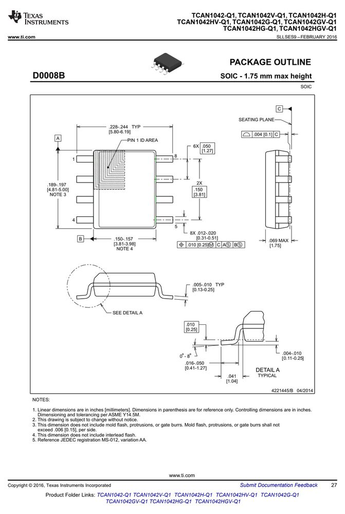
图纸取自原厂规格书,点击可放大查看原始尺寸标注。
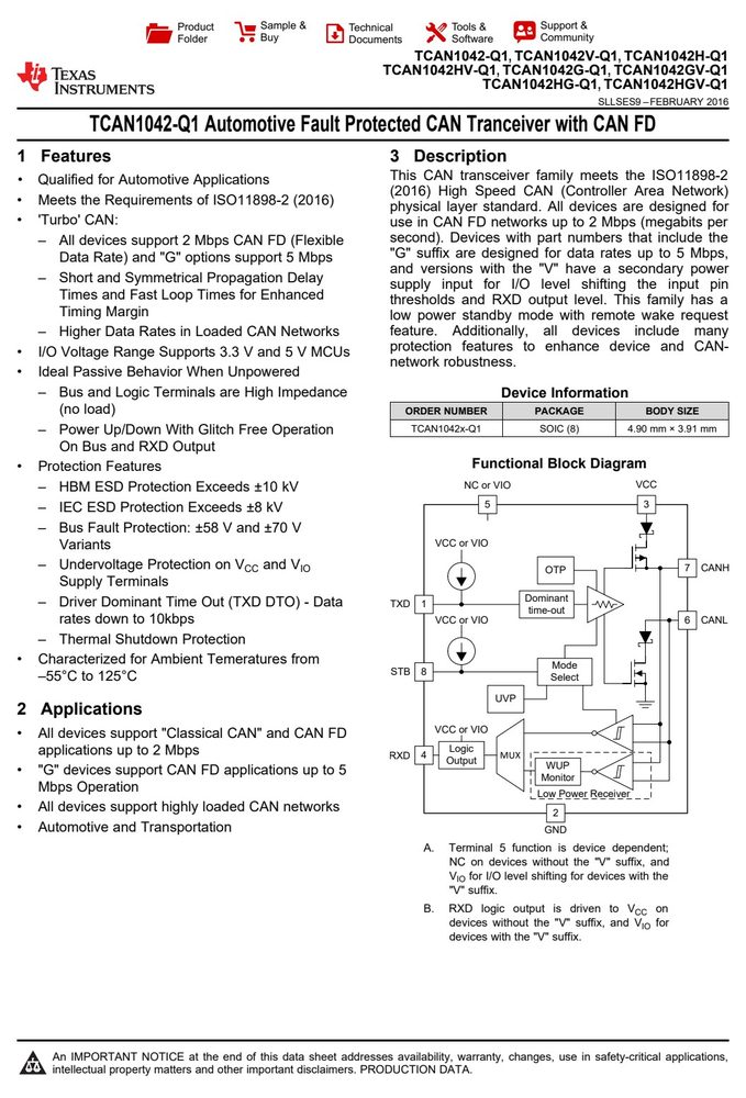
引脚定义与内部结构
| 引脚 | 符号 | 名称 |
|---|---|---|
| 5 | Device Comparison Table | |
| 8 | PIN (SOIC) | |
| 7 | Specifications |
数据来源:原厂规格书引脚图
关键参数速览
- 电源电压 VCC
- 17
产品特点 Features
- This CAN transceiver family meets the ISO11898-2
- I/O Voltage Range Supports 3.3 V and 5 V MCUs network robustness.
- Ideal Passive Behavior When Unpowered
- Bus and Logic Terminals are High Impedance Device Information
- (no load)
- ORDER NUMBER PACKAGE BODY SIZE
- Power Up/Down With Glitch Free Operation TCAN1042x-Q1 SOIC (8) 4.90 mm × 3.91 mm
- On Bus and RXD Output
- TXD_DTO
- Figure 12. Example Timing Diagram for TXD DTO
- TXD_DTO minimum, limits the minimum data rate. Calculate the minimum transmitted data rate by:
- Minimum Data Rate = 11 / t .
- 9.3.2 Thermal Shutdown
- Product Folder Links: TCAN1042-Q1 TCAN1042V-Q1 TCAN1042H-Q1 TCAN1042HV-Q1 TCAN1042G-Q1
- TCAN1042GV-Q1 TCAN1042HG-Q1 TCAN1042HGV-Q1
- TCAN1042-Q1, TCAN1042V-Q1, TCAN1042H-Q1
绝对最大额定值 Absolute Maximum Ratings(TA = 25°C)
超过下表数值可能造成器件永久损坏,设计时请留余量。
| 最小 | 最大 | 单位 |
|---|---|---|
| DEVICE | 5-Mbps FLEXIBLE DATA | 3-V LEVEL SHIFTER |
| NUMBER | RATE | INTEGRATED |
| TCAN1042G-Q1 | ±58 V | X |
| TCAN1042H-Q1 | ±70 V | with Remote Wake |
| TCAN1042HG-Q1 | ±70 V | X |
| TCAN1042HV-Q1 | ±70 V | X |
| TCAN1042-Q1, TCAN1042V-Q1, TCAN1042H-Q1 | ||
| TCAN1042HV-Q1, TCAN1042G-Q1, TCAN1042GV-Q1 | ||
| TCAN1042HG-Q1, TCAN1042HGV-Q1 | ||
| 7 Specifications | ||
| V 5V bus supply voltage range –0.3 V -58 | +7 +58 | |
| I RXD (Receiver) output current -8 | +8 | mA |
| T –55 | 150 | °C |
| TCAN1042-Q1, TCAN1042V-Q1, | TCAN1042H-Q1 | |
| TCAN1042HV-Q1, TCAN1042G-Q1, | TCAN1042GV-Q1 | |
| TCAN1042HG-Q1, | TCAN1042HGV-Q1 |
数据来源:原厂规格书
电气特性 Electrical Characteristics(TA = 25°C)
| 参数 | 测试条件 | 最小 | TYP(1) | 最大 | 单位 |
|---|---|---|---|---|---|
| Over recommended operating conditions | with T = –55°C to 125°C (unless otherwise | noted). | |||
| See Figure 5, TXD = 0 V, R = | 60 Ω, | ||||
| C = open, R = open, STB = | 0 V, | 40 | 70 | ||
| (Driving | Dominant) See Figure 5, TXD = 0 V, R = | 50 Ω, | |||
| C = open, R = open, STB = | 0 V, | 45 | 80 | ||
| Normal | Mode See Figure 5, TXD = 0 V, STB | = 0V, | |||
| (Driving | Dominant – CANH = -12V, R = open, C = | open, | 180 | ||
| See Figure 5, TXD = V or V | , R = | ||||
| Normal | Mode CC IO | L | |||
| I CC 5-V Supply current (Recessive) | 50 Ω, C L = open, R CM = open, | STB = | 1.5 | 2.5 | |
| Shifting Devices), V not needed | in | ||||
| Standby Mode, See Figure 5, | TXD = | 0.5 | 5 | ||
| V , R = 50 Ω, C = open, R | = | ||||
| only), See Figure 5, TXD = V | , R = | µA | |||
| CC | L | 22 | |||
| 50 Ω, C = open, R = open, | STB = | ||||
| Normal | Mode RXD floating, TXD = STB = 0 or | 5.5 V | 90 | 300 | |
| I IO I/O Supply Current Standby | Mode RXD floating, TXD = STB = V IO , | V CC = | 12 | 17 | |
| CC | 4.2 | 4.4 | V | ||
| CC | 3.8 | 4.0 | 4.25 | ||
| V Hysteresis voltage on UV | 200 | mV | |||
| V Hysteresis voltage on UV | 80 | mV | |||
| V HIGH-level input voltage | Shifting Devices) | IO | |||
| V IL LOW-level input voltage | Shifting Devices) | V IO | |||
| I HIGH-level input leakage current | STB = V = V = 5.5 V | -2 | 2 | ||
| I Low-level input leakage current | STB = 0V, V = V = 5.5 V | –20 | 0 | -2 | µA |
| I Unpowered leakage current | STB = 5.5 V, V = V = 0 V | -1 | 0 | 1 | |
| V HIGH level input voltage | Shifting Devices) | IO | |||
| V IL LOW level input voltage | Shifting Devices) | V IO | |||
| I HIGH level input leakage current | TXD = V = V = 5.5 V | –2.5 | 0 | 1 | µA |
| I Low level input leakage current | TXD = 0V, V = V = 5.5 V | –100 | -25 | –7 | µA |
| I Unpowered leakage current | TXD = 5.5 V, V = V = 0 V | –1 | 0 | 1 | µA |
| Product Folder Links: TCAN1042-Q1 | TCAN1042V-Q1 TCAN1042H-Q1 | TCAN1042HV-Q1 | TCAN1042G-Q1 | ||
| TCAN1042-Q1, | TCAN1042V-Q1, | TCAN1042H-Q1 | |||
| TCAN1042HV-Q1, | TCAN1042G-Q1, | TCAN1042GV-Q1 | |||
| TCAN1042HG-Q1, | TCAN1042HGV-Q1 | ||||
| Over recommended operating conditions | with T = –55°C to 125°C (unless otherwise | noted). | |||
| C Input Capacitance | 5 | pF | |||
| Shifting Devices), See Figure 6, | I = 0.8 × V 4 | 4.6 | |||
| Shifting Devices), See Figure 6, | I = | ||||
| V LOW level output voltage | +2 mA. | IO | |||
| I Unpowered leakage current | RXD = 5.5 V, V = 0 V, V = | 0 V –1 | 0 | 1 | µA |
| V | V, STB = 0 V, 50 Ω ≤ R ≤ 65 Ω, | C = | |||
| O(D) (dominant) CANL | open, R = open L | L 0.5 | 2.25 | ||
| Bus output voltage | 0.5 × | ||||
| O(R) (recessive) | CC IO IO CC | L | V | ||
| = open (no load), R = open | CC | ||||
| V, STB = 0 V, 50 Ω ≤ R ≤ 65 Ω, | C = 1.5 | 3 | |||
| V, STB = 0 V, 45 Ω ≤ R < 50 Ω, | C = 1.4 | 3 | |||
| V , STB = 0 V, R = 60 Ω, C | = open, –120 | 12 | |||
| V CANH - | CANL | mV | |||
| V , STB = 0 V, R = open (no | load), –50 | 50 | |||
| V | –0.4 | 0.4 | V | ||
| SYM (V – V – V ) | V, R = 60 Ω, C = open, R = | open | |||
| V, V = 0 V, CANL = open, | TXD = –100 | ||||
| V, V = 32 V, CANH = open, | TXD = | 100 | |||
| Short circuit steady-state output | current, V, –20 V ≤ V ≤ 32 V, Where | V = | |||
| I | BUS | BUS –5 | 5 | mA | |
| OS(SS_REC) Recessive V V | CANH = CANL, TXD = V , | Normal 500 | 900 | ||
| V V V IT+ IT– | 400 | 120 | 1000 | mV | |
| Product Folder Links: TCAN1042-Q1 | TCAN1042V-Q1 TCAN1042H-Q1 | TCAN1042HV-Q1 | TCAN1042G-Q1 | ||
| Over recommended operating conditions | with T = –55°C to 125°C (unless otherwise | noted). -12 | 12 | ||
| CM Common mode range, standby | mode Shifting Devices), See Figure 6, | -2 | +7 | V | |
| V Input threshold voltage, standby | mode STB = V or V | 400 | 1150 | mV | |
| I | CANH = CANL = 5 V, V = V | = 0 V | 6 | µA | |
| Input capacitance to ground | (CANH or TXD = V , V = V , V = 0.4 | sin | |||
| C | CC IO CC I | 24 | 30 | ||
| Differential input capacitance | (CANH to TXD = V , V = V , V = 0.4 | sin | |||
| C | CC IO CC I | 12 | 15 | ||
| R Differential input resistance | 30 | 80 | |||
| TXD = V = V = 5 V, STB = | 0 V | kΩ | |||
| R Input resistance (CANH or CANL) | 15 | 40 | |||
| R | V = V | –2% | 2% | ||
| Product Folder Links: TCAN1042-Q1 | TCAN1042V-Q1 TCAN1042H-Q1 | TCAN1042HV-Q1 | TCAN1042G-Q1 | ||
| TCAN1042-Q1, | TCAN1042V-Q1, | TCAN1042H-Q1 | |||
| TCAN1042HV-Q1, | TCAN1042G-Q1, | TCAN1042GV-Q1 | |||
| TCAN1042HG-Q1, | TCAN1042HGV-Q1 |
特性曲线(Typical Performance Curves)