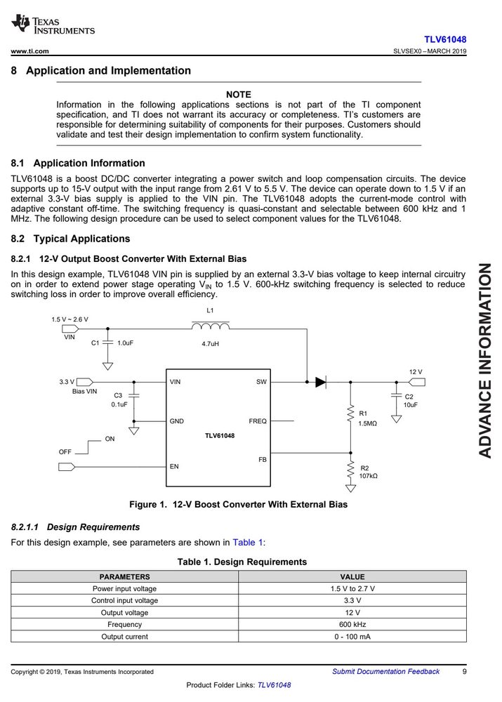
产品应用与封装尺寸
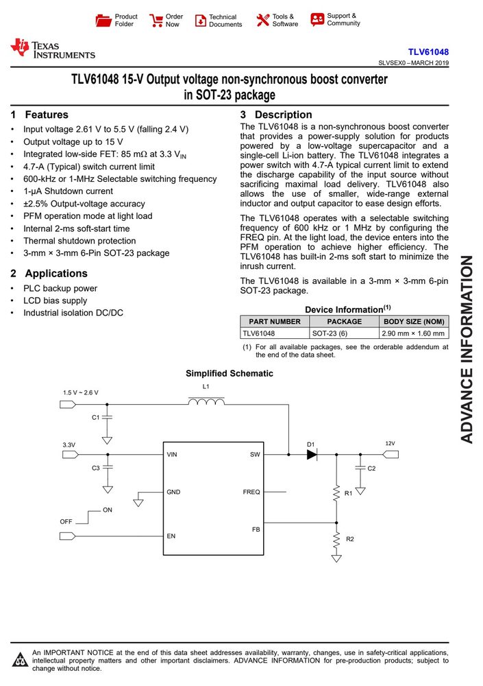
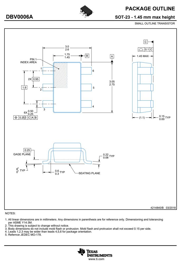
图纸取自原厂规格书,点击可放大查看原始尺寸标注。
引脚定义与内部结构
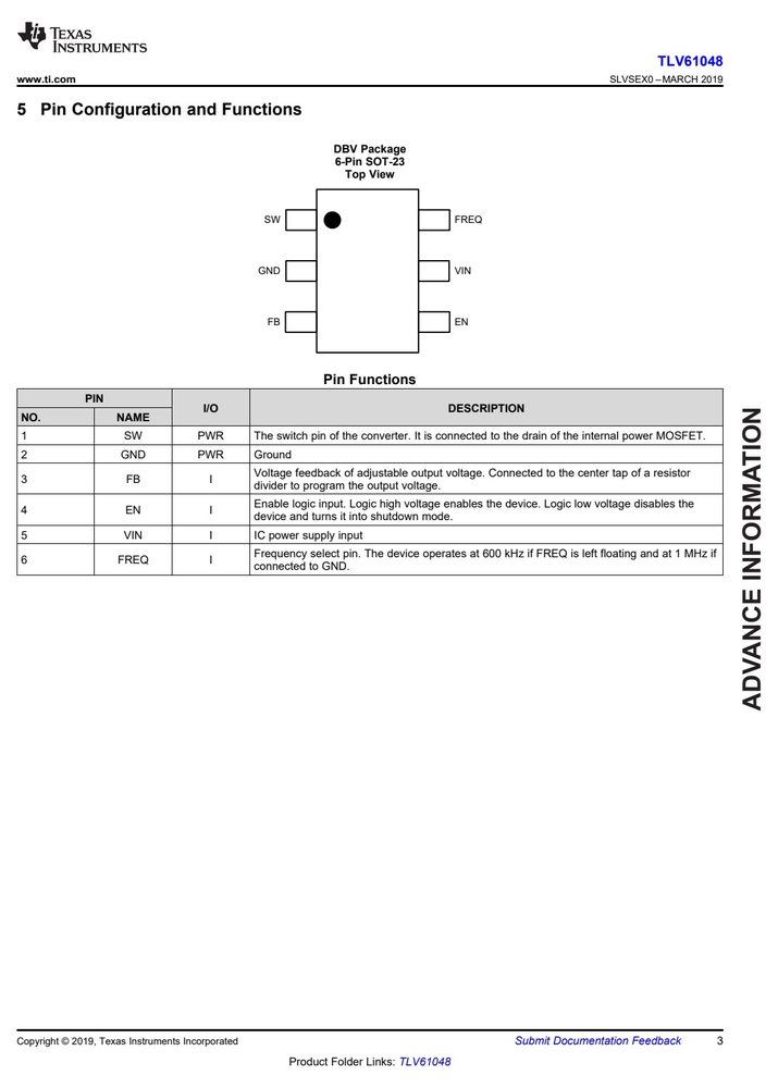
| 引脚 | 符号 | 名称 |
|---|---|---|
| 1 | SW | |
| 2 | GND | |
| 3 | FB | |
| 4 | EN | |
| 5 | VIN | |
| 6 | FREQ |
数据来源:原厂规格书引脚图
产品特点 Features
- The TLV61048 is a non-synchronous boost converter
- Input voltage 2.61 V to 5.5 V (falling 2.4 V)
- 1 that provides a power-supply solution for products
- Output voltage up to 15 V powered by a low-voltage supercapacitor and a
- Integrated low-side FET: 85 mΩ at 3.3 V single-cell Li-ion battery. The TLV61048 integrates a
- 4.7-A (Typical) switch current limit power switch with 4.7-A typical current limit to extend the discharge capability of the input source without
- 600-kHz or 1-MHz Selectable switching frequency sacrificing maximal load delivery. TLV61048 also
- 1-µA Shutdown current allows the use of smaller, wide-range external
- ±2.5% Output-voltage accuracy inductor and output capacitor to ease design efforts.
- PFM operation mode at light load
- The TLV61048 operates with a selectable switching
- Internal 2-ms soft-start time frequency of 600 kHz or 1 MHz by configuring the
- FREQ pin. At the light load, the device enters into the
- Thermal shutdown protection
- PFM operation to achieve higher efficiency. The
- 3-mm × 3-mm 6-Pin SOT-23 package
绝对最大额定值 Absolute Maximum Ratings(TA = 25°C)
超过下表数值可能造成器件永久损坏,设计时请留余量。
| 最小 | 最大 | 单位 |
|---|---|---|
| TLV61048 | ||
| 6 Specifications | ||
| over operating free-air temperature range (unless otherwise noted) (1) | ||
| VIN, EN, FREQ – 0.3 | 6 | V |
| Voltage range at terminals (2) SW –0.3 | 18 | V |
| FB -0.3 | 3.6 | V |
| Operating junction temperature range, T –40 | 150 | °C |
| (2) All voltage values are with respect to network ground terminal. |
数据来源:原厂规格书
电气特性 Electrical Characteristics(TA = 25°C)
| 参数 | 测试条件 | 最小 | 典型 | 最大 | 单位 |
|---|---|---|---|---|---|
| T = –40°C to 85°C, V = 3.3 V. Typical | values are at T = 25°C, unless otherwise | noted. | |||
| V Input voltage range | 2.6 | 5.5 | V | ||
| V rising | 2.55 | 2.61 | |||
| V falling | 2.3 | 2.4 | |||
| V VIN UVLO hysteresis | 150 | mV | |||
| I Quiescent current into VIN pin | IC enabled, no load, no switching | 100 | µA | ||
| I Shutdown current into VIN pin | IC disabled, V = 2.6 V to 5.5 V, T = 25°C | 1.0 | µA | ||
| V Output voltage range | 3.3 | 15 | V | ||
| PWM mode, T =-40°C to 125°C | 0.78 | 0.8 | 0.82 | V | |
| PFM mode, T =25°C | 0.81 | V | |||
| I Leakage current into FB pin | T = 25°C | 50 | nA | ||
| I Leakage current into SW pin | IC disabled, SW = 5.5V | 500 | nA | ||
| R Low-side MOSFET on resistance | Vin = 3.3, Vout = 12V | 85 | mΩ | ||
| Default, SW = 1.5V | 480 | 550 | 620 | kHz | |
| Default, SW = 2.6V | 1020 | 1150 | 1280 | kHz | |
| tOFF_min Min. off time | 600kHz, SW = 1.5V | 130 | ns T | ||
| I Peak switch current limit | 600kHz, V = 3.3V | 3.8 | 4.7 | 5.6 | A |
| t Startup time | 2 | ms M | |||
| V EN_H EN Logic high threshold | 1.2 | V O | |||
| V EN Logic low threshold | 0.4 | V | |||
| R EN EN Pull Down Resistor | 1 | MΩ N | |||
| R FREQ pull up resistance | 800 | kΩ | |||
| V FREQ logic high threshold | 1.2 | V E | |||
| V FREQ logic low threshold | 0.4 | V C | |||
| T SD Thermal shutdown threshold | T J rising | 150 | °C A | ||
| T SD_HYS Thermal shutdown hysteresis | T J falling below T SD | 20 | °C V |
特性曲线(Typical Performance Curves)