
引脚定义与内部结构
| 引脚 | 符号 | 名称 |
|---|---|---|
| 8 | 3A | |
| 9 | 3B | |
| 10 | 3Y | |
| 11 | 4A | |
| 12 | 4B | |
| 13 | 4Y | |
| 14 | VCC |
数据来源:原厂规格书引脚图
关键参数速览
- 正向电流 IF
- [1] The input
产品特点 Features
- Wide supply voltage range from 2.0 V to 6.0 V
- CMOS low power dissipation
- High noise immunity
- Latch-up performance exceeds 100 mA per JESD 78 Class II Level B
- Input levels:
- For 74HC02: CMOS level
- For 74HCT02: TTL level
- Complies with JEDEC standards:
绝对最大额定值 Absolute Maximum Ratings(TA = 25°C)
超过下表数值可能造成器件永久损坏,设计时请留余量。
| 符号 | 参数 | 条件 |
|---|---|---|
| I | input clamping current | V < -0.5 V or |
| I | output clamping current | V < -0.5 V or |
| I | output current | -0.5 V < V < |
| P | total power dissipation | SOT108-1 SOT402-1 SOT762-1 |
| [2] For | SOT108-1 (SO14) package: P | derates linearly with 10.1 |
| For | SOT402-1 (TSSOP14) package: | P derates linearly with 7.3 |
| For | SOT762-1 (DHVQFN14) package: | P derates linearly with -0.5 +7 V |
| > V + 0.5 V [1] - ±20 mA | ||
| V > V + 0.5 V [1] - ±20 mA | ||
| + 0.5 V - ±25 mA - 50 mA -50 - mA -65 +150 °C [2] - 500 mW - 250 mW | ||
| above 100 °C. above 81 °C. | ||
| mW/K above 98 °C. |
数据来源:原厂规格书
相关 / 可替代型号
以上型号来自规格书与型号命名比对,参数需以各自规格书为准;下单前请与销售确认封装与脚位。
应用领域 Applications
产品应用与封装尺寸
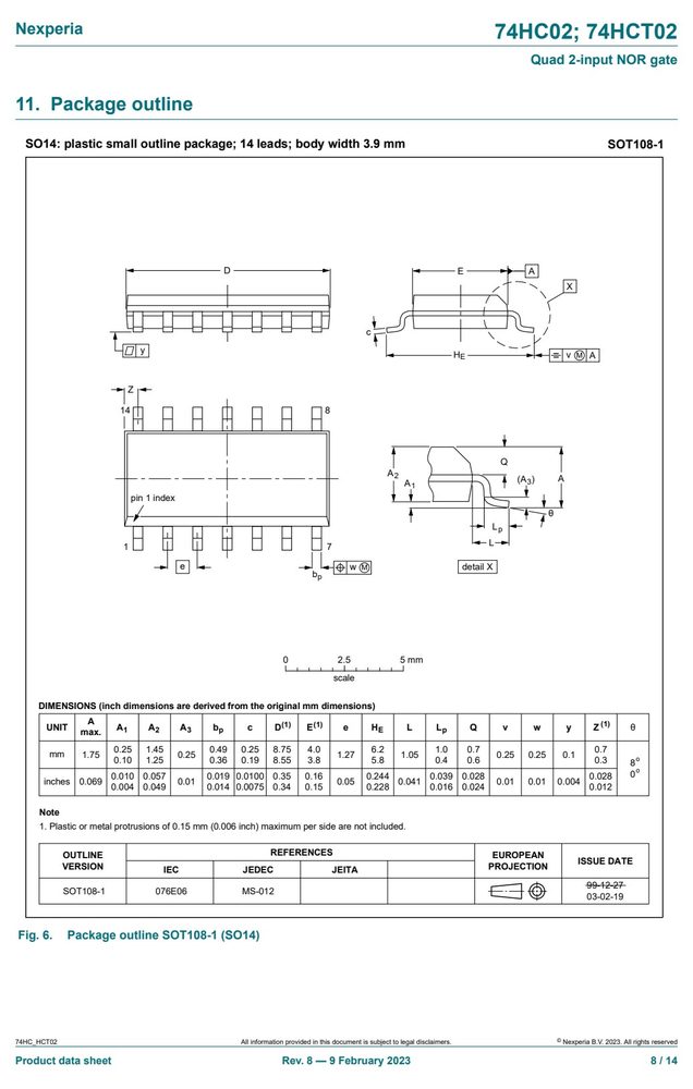
图纸取自该型号原厂规格书的应用电路与封装尺寸章节,点击图片可放大查看原始尺寸标注。