
产品应用与封装尺寸
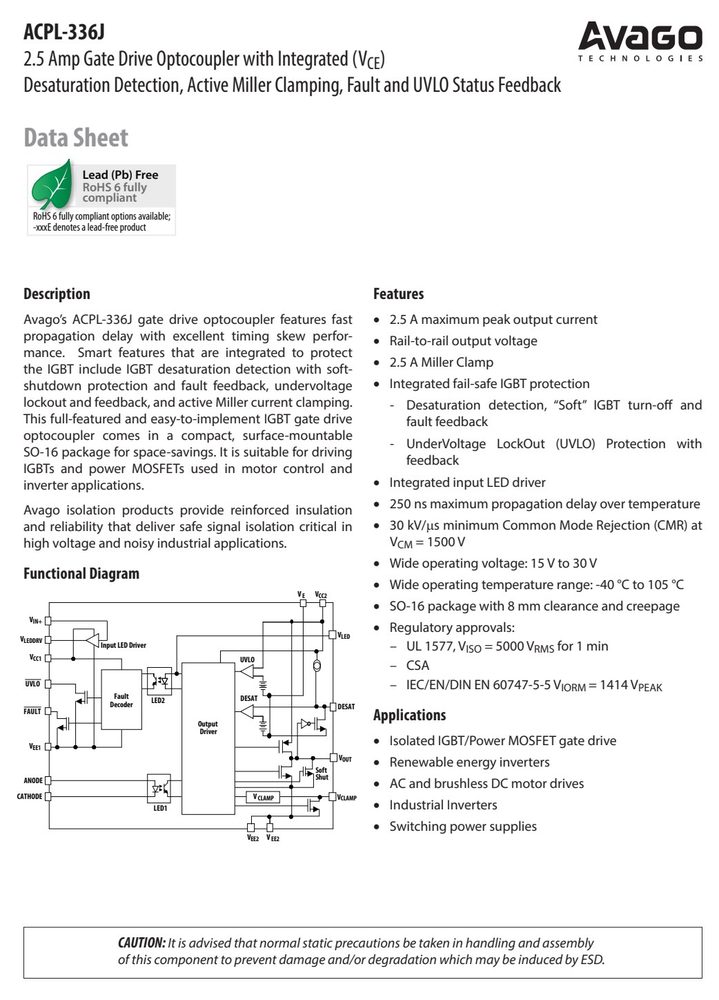
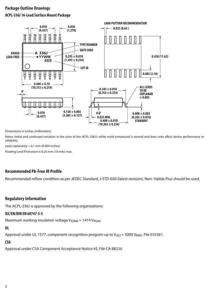
图纸取自原厂规格书,点击可放大查看原始尺寸标注。
引脚定义与内部结构
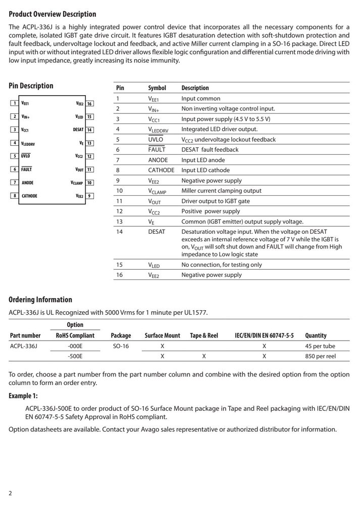
| 引脚 | 符号 | 名称 |
|---|---|---|
| 1 | V Input common | |
| 6 | FAULT DESAT fault feedback | |
| 7 | ANODE Input LED anode | |
| 9 | V Negative power supply | |
| 12 | V Positive power supply | |
| 16 | V Negative power supply |
数据来源:原厂规格书引脚图
关键参数速览
- 正向电压 VF
- 4
- 电源电压 VCC
- voltage (VCC2
- 工作温度 TA
- 105
产品特点 Features
- Avago’s ACPL-336J gate drive optocoupler features fast • 2.5 A maximum peak output current propagation delay with excellent timing skew perfor-
- Rail-to-rail output voltage
- UnderVoltage LockOut (UVLO) Protection with
- SO-16 package for space-savings. It is suitable for driving feedback
- IGBTs and power MOSFETs used in motor control and
绝对最大额定值 Absolute Maximum Ratings(TA = 25°C)
超过下表数值可能造成器件永久损坏,设计时请留余量。
| 参数 | 符号 | 最小 | 最大 | 单位 | 备注 |
|---|---|---|---|---|---|
| Storage Temperature | T | -55 | 125 | °C | |
| Operating Temperature | T | -40 | 105 | °C | |
| Output IC Junction Temperature | T | 125 | °C | ||
| Average Input Current | I | 20 | mA | 1 | |
| Peak Transient Input Current | I | 1 | A | ||
| Peak Output Current | |I | | 2.5 | A | 2 | |
| FAULT Output Current | I | 10 | mA | ||
| FAULT Pin Voltage | V FAULT | -0.5 | V CC1 | V | |
| UVLO Output Current | I | 10 | mA | ||
| UVLO Pin Voltage | V UVLO | -0.5 | V CC1 | V | |
| Non Inverting Voltage Control | Input Voltage V IN+ | -0.5 | V CC1 | V | |
| Integrated LED Driver Output | Current I | 20 | mA | ||
| Integrated LED Driver Output | Voltage V LEDDRV | -0.5 | V CC1 | V | |
| Positive Input Supply Voltage | V | -0.5 | 7.0 | V | |
| Total Output Supply Voltage | V – V | -0.5 | 35 | V | |
| Negative Output Supply Voltage | V – V | -0.5 | 15 | V | 3 |
| Positive Output Supply Voltage | V – V | -0.5 | 35 – (V – V | ) V | |
| CC2 E | E | EE | |||
| Gate Drive Output Voltage | V O(PEAK) | -0.5 | V CC2 | V | |
| Peak Clamping Sinking Current | I | 2.5 | A | 2 | |
| Miller Clamping Pin Voltage | V CLAMP | -0.5 | V CC2 | V | |
| DESAT Voltage | V | V – 0.5 | (V + 0.5) | V | |
| DESAT | E | CC2 | |||
| Output IC Power Dissipation | P | 600 | mW | 4 | |
| Input LED Power Dissipation | P | 150 | mW | 5 |
数据来源:原厂规格书
安全与绝缘额定值(DIN EN/IEC 60747−5−5)
| 型号 | 型号2 |
|---|---|
| Approval under UL 1577, component recognition | program up to V = 5000 V . File E55361. |
| Approval under CSA Component Acceptance Notice 30 - - V | #5, File CA 88324. 0.5 I = -100 mA CC2 EE2 |
| Figure 5. V vs. temperature 160 - 120 80 | Figure 6. V vs. temperature 7.5 - 7 |
| WOL- GNIRUD 40 -40 I 0 -0.80 -0.85 -0.90 | - 6.8 TASED 6.7 6.6 6.5 80 - 70 60 |
| -0.95 -1.00 -1.05 -1.10 | GNIGRAHCSID 50 40 30 20 |
| GHC -1.15 -1.20 200 180 | - 10 I 0 250 230 F |
| sn 160 | sn 210 DUTY CYCLE = 50% |
| - YALED 140 120 100 80 60 0 | - YALED 190 f = 10 kHz 170 150 130 110 50 |
| Figure 11. Propagation delay vs. temperature - | Figure 12. Propagation delay vs. supply voltage f = 10 kHz |
| 1 V EE1 | V EE2 16 |
| 2 V IN+ | V LED 15 |
| 3 V CC1 | DESAT 14 |
| 4 V LEDDR V OUT 150Ω 5 V | V E 13 30 V 10 nF _ |
电气特性 Electrical Characteristics(TA = 25°C)
| 参数 | 符号 | 最小 | 典型 | 最大 | 单位 | 测试条件 | 图号 | 备注 |
|---|---|---|---|---|---|---|---|---|
| Unless otherwise noted, | all typical values | at T = 25 | °C, V | = 5 V, V | – V | = 30 V, V – V | = 0 V; all | Minimum/ |
| A | CC1 | CC2 | EE2 | E EE2 | ||||
| Maximum specifications | are at Recommended | Operating | Conditions. | |||||
| Logic Low Input Voltage | V | 0.8 | V | 23 | ||||
| Logic High Input Voltage | V | 2 | V | 23 | ||||
| Logic High LED Driver | Output R R | 5.5 | 13.5 | 24 | W | I = -10 mA, V | = 5 V 23 | |
| DS(ON) LEDDRVH | LEDDRV | IN+ | ||||||
| Logic Low LED Driver | Output Voltage V | 0.2 | 0.4 | 0.8 | V | I = 2.4 mA, V | = 0 V 23 | |
| LEDDRVL | LEDDRV | IN+ | ||||||
| Input Low Supply Current | I CC1L | 3 | 6 | mA | I = 0 mA, V = 0 V F IN+ | 1 | ||
| Input High Supply Current | I CC1H | 3 | 6 | mA | I = 10 mA, V =0 V F IN+ | 1 | ||
| 13 | 16 | mA | I = 10 mA , V | =5 V | ||||
| Output Low Supply | Current I CC2L | 4.3 | 6.5 | mA | I = 0 mA F | 2, 3 | ||
| Output High Supply | Current I CC2H | 5.4 | 7.5 | mA | I = 10 mA F | 2, 3 | ||
| LED Forward Voltage | V | 1.2 | 1.55 | 1.95 | V | I =10 mA | 4 | |
| Temperature Coefficient | of Input ΔV /ΔT | -1.7 | mV/°C | I = 10 mA | ||||
| Input Capacitance | C | 70 | pF | |||||
| LED Turn on Current | Threshold Low I | 0.25 | 2 | 6 | mA | V = 5 V | ||
| LED Turn on Current | Threshold High I | 0.15 | 1.5 | 5.5 | mA | V = 5 V | ||
| LED Turn on Current | Hysteresis I | 0.5 | mA | |||||
| High Level Output Current | I OH | -2 | -3.5 | A | V - V =15 V CC2 OUT | 1 | ||
| Low Level Output Current | I OL | 2 | 3.0 | A | V - V = 15 V OUT EE | 1 | ||
| High Output Transistor | R R | 0.5 | 2.5 | 5.0 | W | I = -2 A | 2 | |
| Low Output Transistor R | R | 0.2 | 1.8 | 4.0 | W | I = 2 A | 2 | |
| Low Level Output Current | During I OLF | 55 | 115 | 170 | mA | V - V = 14 V OUT EE | 7 | 3 |
| High Level Output Voltage | V | V – | 0.5 V – | 0.15 | V | I = -100 mA | 5 | 4, 5, 6 |
| OH | CC2 | CC2 | OUT | |||||
| Low Level Output Voltage | V | 0.1 | 0.5 | V | I = 100 mA | 6 | ||
| Clamp Threshold Voltage | V | 2 | 3 | V | ||||
| Clamp Low Level Sinking | Current I | 0.75 | 1.9 | A | V = V + 2.5 | |||
| CLAMP | CLAMP EE | |||||||
| Clamp Output Transistor | R R | 1.1 | 3.5 | W | I = 1 A | |||
| V UVLO Threshold | Low to High V | 11 | 12.5 | 13.7 | V | V > 5 V | 4, 6, 7 | |
| CC2 | UVLO+ | OUT | ||||||
| V UVLO Threshold | High to Low V | 10.1 | 11.3 | 12.8 | V | V < 5 V | 4, 6, 8 | |
| CC2 | UVLO- | OUT | ||||||
| V UVLO Hysteresis | V | 0.4 | 1.2 | V | ||||
| DESAT Detection Threshold | V | 6.2 | 7 | 7.8 | V | 8 | 6 | |
| DESAT Charging Current | I | 0.6 | 1.0 | 1.2 | mA | V = 2 V | 9 | 6, 9 |
| DESAT Discharging Current | I | 20 | 58 | mA | V = 8 V | 10 | ||
| FAULT Logic Low Output | Current I | 4 | 9.0 | mA | V = 0.4 V | |||
| FAULT Logic High Output | Current I | 20 | µA | V = 5 V | ||||
| UVLO Logic Low Output | Current I | 4 | 9.0 | mA | V = 0.4 V | |||
| UVLO Logic High Output | Current I | 20 | µA | V = 5 V | ||||
| 2. Output is sourced at -2.0 | A/2.0 A with a maximum | pulse width | = 10 µs. |