
产品实拍图
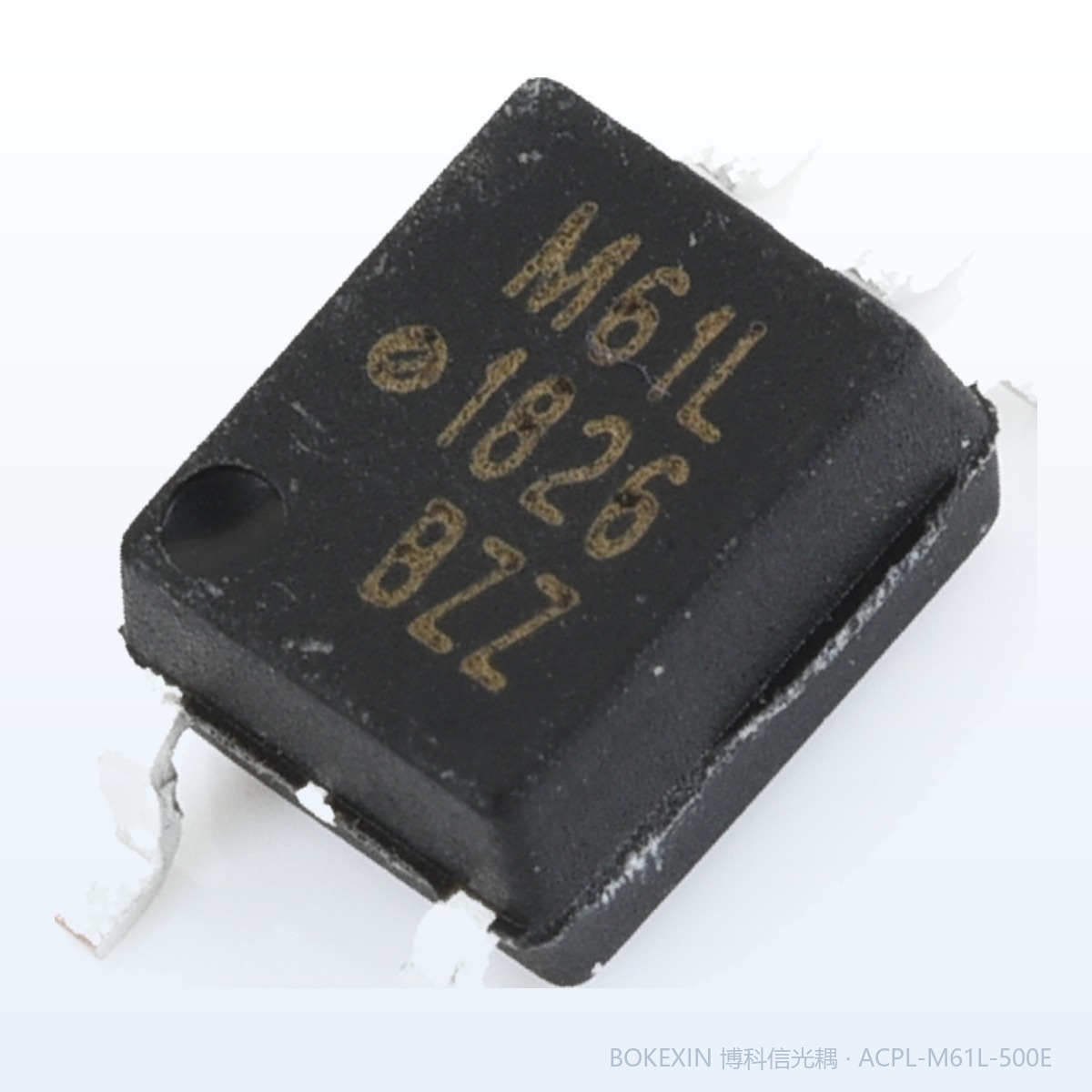
本页为博科信现货实拍(器件丝印 见规格书)。图片已加防盗水印,需要最新批次照片或未加水印原图请联系销售;点击图片可放大。
产品应用与封装尺寸
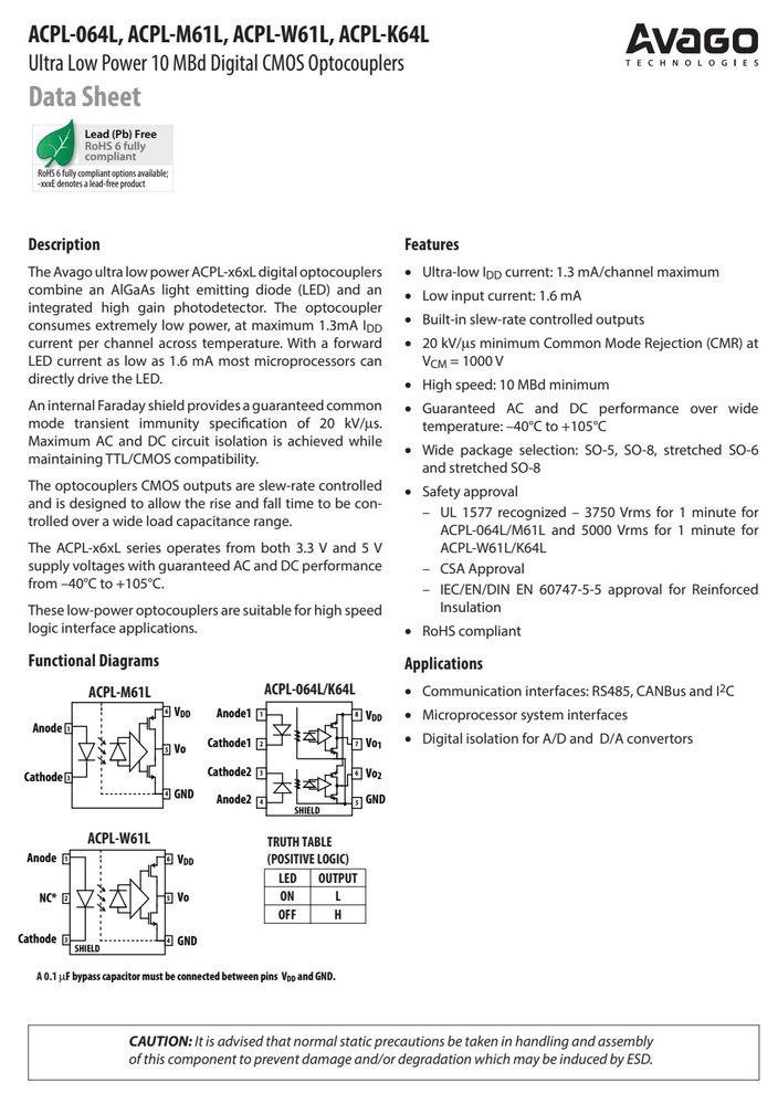
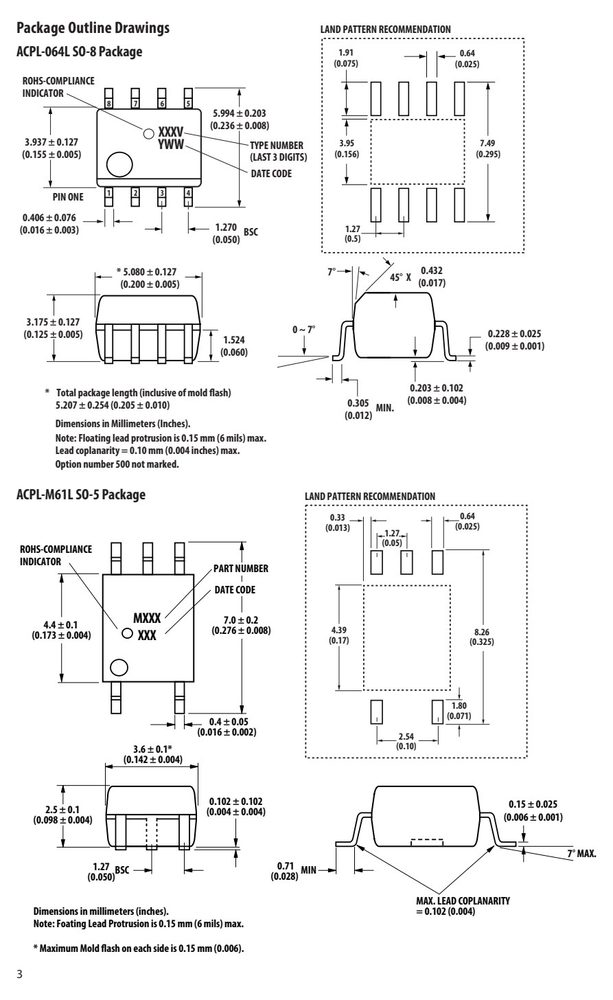
图纸取自原厂规格书,点击可放大查看原始尺寸标注。
关键参数速览
- 正向电压 VF
- 1.7
- 电源电压 VCC
- (2.7 V ≤
- 工作温度 TA
- 105
产品特点 Features
- The Avago ultra low power ACPL-x6xL digital optocouplers • Ultra-low I current: 1.3 mA/channel maximum combine an AlGaAs light emitting diode (LED) and an
- Low input current: 1.6 mA integrated high gain photodetector. The optocoupler
- Built-in slew-rate controlled outputs consumes extremely low power, at maximum 1.3mA I current per channel across temperature. With a forward • 20 kV/μs minimum Common Mode Rejection (CMR) at
- LED current as low as 1.6 mA most microprocessors can V = 1000 V directly drive the LED.
- High speed: 10 MBd minimum
- An internal Faraday shield provides a guaranteed common • Guaranteed AC and DC performance over wide mode transient immunity specification of 20 kV/μs. temperature: –40°C to +105°C
- Maximum AC and DC circuit isolation is achieved while
- Wide package selection: SO-5, SO-8, stretched SO-6 maintaining TTL/CMOS compatibility.
- and stretched SO-8
- The optocouplers CMOS outputs are slew-rate controlled
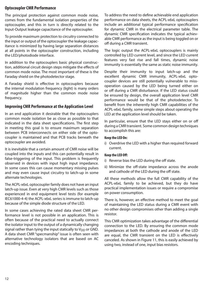
- In addition to the optocouplers basic physical construc- tion, additional circuit design steps mitigate the effects of common mode noise. The most important of these is the
- Faraday shield on the photodetector stage.
- A Faraday shield is effective in optocouplers because the internal modulation frequency (light) is many orders of magnitude higher than the common mode noise frequency.
- Improving CMR Performance at the Application Level
- In some cases this can cause momentary missing pulses and may even cause input circuitry to latch-up in some alternate technologies.
- The ACPL-x6xL optocoupler family does not have an input latch-up issue. Even at very high CMR levels such as those experienced in end equipment level tests (for example
绝对最大额定值 Absolute Maximum Ratings(TA = 25°C)
超过下表数值可能造成器件永久损坏,设计时请留余量。
| 参数 | 符号 | 最小 | 最大 | 单位 | 条件 |
|---|---|---|---|---|---|
| Storage Temperature | T | -55 | 125 | °C | |
| Operating Temperature | T | -40 | 105 | °C | |
| Supply Voltage | V | 6.5 | V | ||
| Average Forward Input | Current I | – | 8 | mA | |
| Peak Forward Input Current | I | – | 1 | A | ≤1 μs Pulse Width, <300 pulses per second |
| F | 80 | mA | ≤1 μs Pulse Width, <10% Duty Cycle | ||
| Output Current | I | 10 | mA | ||
| Output Voltage | V | –0.5 | V +0.5 | V | |
| Input Power Dissipation | P | 14 | mW | ||
| Output Power Dissipation | P | 20 | mW | ||
| Lead Solder Temperature | T | 260°C for | 10 sec., 1.6 | mm below seating plane |
数据来源:原厂规格书
安全与绝缘额定值(DIN EN/IEC 60747−5−5)
| 参数 | 符号 | ACPL-064L | ACPL-M61L | ACPL-K64L | 单位 | 条件 |
|---|---|---|---|---|---|---|
| ACPL-W61L | ||||||
| Minimum External | L(101) | 4.9 | 5 | 8 | mm | Measured from input terminals to output |
| Air Gap | terminals, shortest distance through air. | |||||
| Minimum External | L(102) | 4.8 | 5 | 8 | mm | Measured from input terminals to output |
| Tracking | terminals, shortest distance path along body. | |||||
| Plastic Gap | conductor, usually the straight line distance | |||||
| (Internal Clearance) | thickness between the emitter and detector. | |||||
| Tracking Resistance | CTI | 175 | 175 | 175 | V | DIN IEC 112/VDE 0303 Part 1 |
| Isolation Group | IIIa | IIIa | IIIa | Material Group | ||
| (DIN VDE 0110, 1/89, Table 1) |
电气特性 Electrical Characteristics(TA = 25°C)
| 参数 | 符号 | Channel | 最小 | 典型 | 最大 | 单位 | 测试条件 |
|---|---|---|---|---|---|---|---|
| Input Forward | Voltage V | 0.95 | 1.3 | 1.7 | V | I = 2 mA Figure 1, 2 | |
| Logic High | V | V - 0.1 | V | V | I = 0 mA, V = 0 V (R = 1.68 kΩ) | ||
| OH | DD | DD | F I T | ||||
| Output Voltage | or (R = 870 Ω), I = -20 μA | ||||||
| V - 1.0 | V | V | I = 0 mA, V = 0 V (R = 1.68 kΩ) | ||||
| DD | DD | F I T | |||||
| or (R = 870 Ω), I = -3.2 mA | |||||||
| Logic Low | V OL | 0.03 | 0.1 | V | I = 2 mA, V = 5 V (R = 1.68 kΩ) F I T | ||
| Output Voltage | or V = 3.3V (R = 870 Ω), I = 20 μA | ||||||
| 0.18 | 0.4 | V | I = 2 mA, V = 5 V (R = 1.68 kΩ) | ||||
| or V = 3.3V (R = 870 Ω), I = 3.2 mA | |||||||
| Input Threshold | Current I | 0.7 | 1.3 | mA | Figure 3 | ||
| Logic Low Output | I | Single | 0.8 | 1.3 | mA | Figure 4 | |
| Dual | 1.6 | 2.6 | |||||
| Logic High Output | I | Single | 0.8 | 1.3 | mA | Figure 5 | |
| Dual | 1.6 | 2.6 | |||||
| Input Capacitance | C | 60 | pF | f = 1 MHz, V = 0 V | |||
| Input Diode | ΔV /ΔT | -1.6 | mV/°C | I = 2 mA |
特性曲线(Typical Performance Curves)
订货信息与供货形式
| 型号 | 型号2 | RoHS | Compliant | 封装 | Mount | & | 包装 | 额定值 | 60747-5-5 | 数量 |
|---|---|---|---|---|---|---|---|---|---|---|
| devices | are | RoHS | compliant. | |||||||
| option | from | the option | column. |