
产品应用与封装尺寸
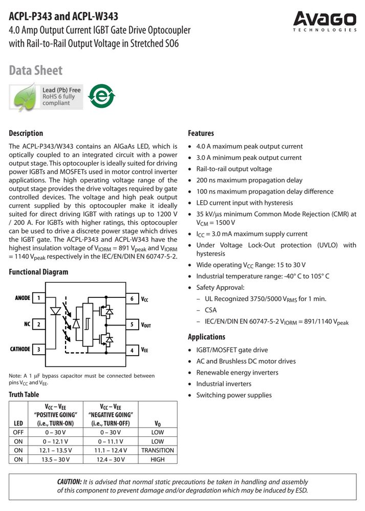
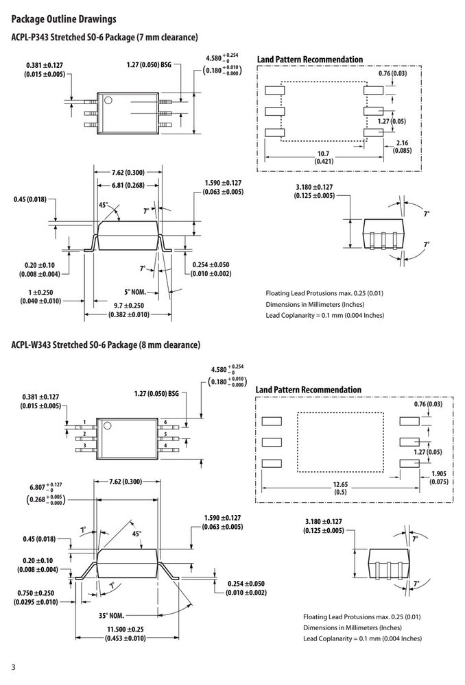
图纸取自原厂规格书,点击可放大查看原始尺寸标注。
关键参数速览
- 电源电压 VCC
- 35
- 工作温度 TA
- 105
产品特点 Features
- The ACPL-P343/W343 contains an AlGaAs LED, which is 4.0 A maximum peak output current optically coupled to an integrated circuit with a power
- 3.0 A minimum peak output current output stage. This optocoupler is ideally suited for driving
- 100 ns maximum propagation delay diff erence controlled devices. The voltage and high peak output
- LED current input with hysteresis current supplied by this optocoupler make it ideally suited for direct driving IGBT with ratings up to 1200 V 35 kV/s minimum Common Mode Rejection (CMR) at
- / 200 A. For IGBTs with higher ratings, this optocoupler V = 1500 V can be used to drive a discrete power stage which drives
- I CC = 3.0 mA maximum supply current the IGBT gate. The ACPL-P343 and ACPL-W343 have the
- Under Voltage Lock-Out protection (UVLO) with
- This thermal model assumes that an 6-pin single-channel cient gate voltage to the IGBT by forcing the ACPL-P343/ plastic package optocoupler is soldered into a 7.62 cm x
- W343 output low during power-up. IGBTs typically require
- 7.62 cm printed circuit board (PCB) per JEDEC standards.
- gate voltages of 15 V to achieve their rated V voltage.
- CE(ON) The temperature at the LED and Detector junctions of
- At gate voltages below 13 V typically, the V voltage
- CE(ON) the optocoupler can be calculated using the equations increases dramatically, especially at higher currents. At below.
- very low gate voltages (below 10 V), the IGBT may operate in the linear region and quickly overheat. The UVLO T 1 = (R 11 * P 1 + R 12 * P 2 ) + Ta (1) function causes the output to be clamped whenever
- T = (R * P + R * P ) + Ta (2)
绝对最大额定值 Absolute Maximum Ratings(TA = 25°C)
超过下表数值可能造成器件永久损坏,设计时请留余量。
| 参数 | 符号 | 最小 | 最大 | 单位 | 备注 |
|---|---|---|---|---|---|
| Storage Temperature | T | -55 | 125 | °C | |
| Operating Temperature | T | -40 | 105 | °C | |
| Output IC Junction Temperature | T | 125 | °C | ||
| Average Input Current | I | 25 | mA | 1 | |
| Peak Transient Input Current | I | 1 | A | ||
| “High” Peak Output Current | I | 4.0 | A | 2 | |
| “Low” Peak Output Current | I | 4.0 | A | 2 | |
| Total Output Supply Voltage | (V - V ) | 0 | 35 | V | |
| Input Current (Rise/Fall Time) | t / t | 500 | ns | ||
| Output Voltage | V | -0.5 | V | V | |
| Output IC Power Dissipation | P | 700 | mW | 3 | |
| Total Power Dissipation | P | 745 | mW | 4 | |
| Lead Solder Temperature | 260° C for | 10 sec., 1.6 mm | below seating | plane |
数据来源:原厂规格书
安全与绝缘额定值(DIN EN/IEC 60747−5−5)
| 说明 | 符号 | 包装 | 060 | 包装2 | 0602 | 单位 |
|---|---|---|---|---|---|---|
| ISO | RMS | ISO | RMS | |||
| Maximum Working Insulation Voltage | V = 891 V (ACPL-P343) and | V = | 1140 V | (ACPL-W343) | ||
| IORM peak | IORM | peak | ||||
| ACPL-P343 | ACPL-W343 | |||||
| for rated mains voltage ≤ 150 V | I – IV | I – IV | ||||
| for rated mains voltage ≤ 300 V | I – IV | I – IV | ||||
| for rated mains voltage ≤ 450 V | I – III | I – IV | ||||
| for rated mains voltage ≤ 600 V | I – III | I – IV | ||||
| for rated mains voltage ≤ 1000 V | I – III | |||||
| Pollution Degree (DIN VDE 0110/1.89) | 2 | 2 | ||||
| Input to Output Test Voltage, Method | b* V | 1671 | 2137 | V | ||
| Input to Output Test Voltage, Method | a* V | 1426 | 1824 | V | ||
| Highest Allowable Overvoltage | V | 6000 | 8000 | V |
订货信息与供货形式
| 型号 | 型号2 | RoHS | Compliant |
|---|---|---|---|
| Part | number | RoHS | Compliant |
| column Example | to form 1: | an order | entry. |