
产品应用与封装尺寸
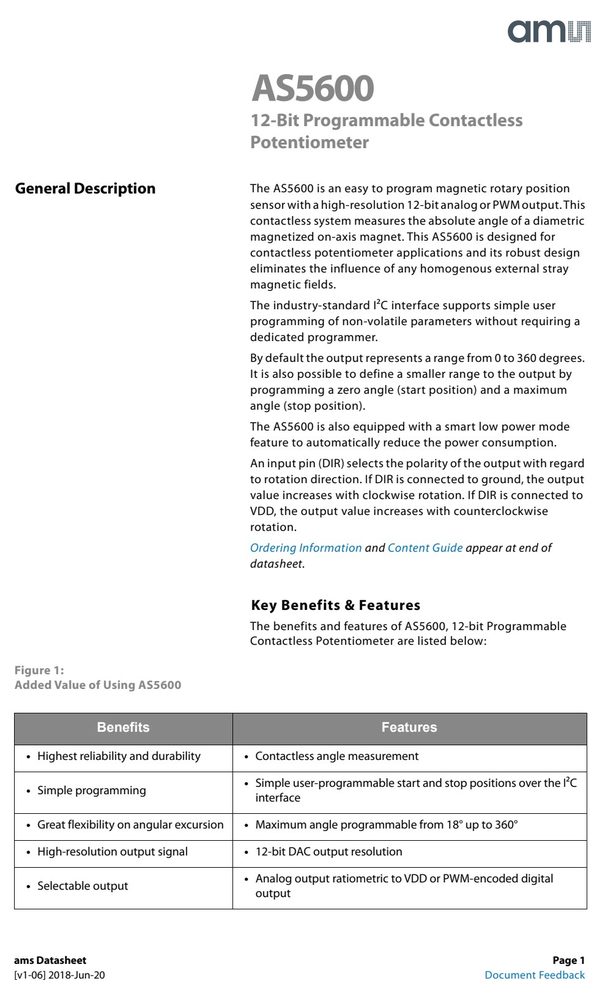
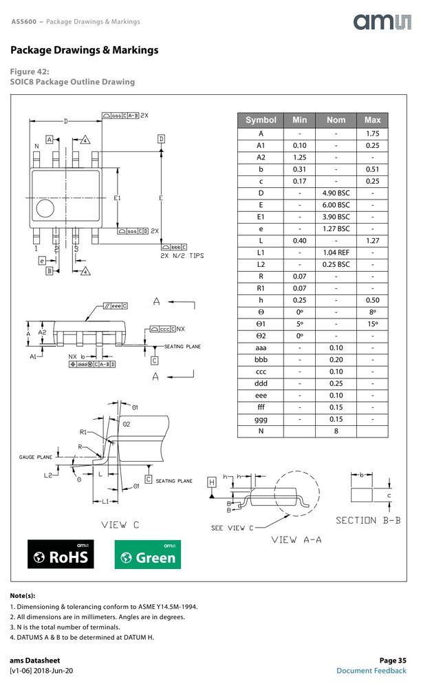
图纸取自原厂规格书,点击可放大查看原始尺寸标注。
引脚定义与内部结构
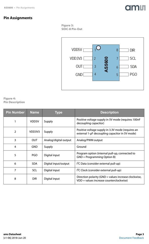
| 引脚 | 符号 | 名称 |
|---|---|---|
| 3 | OUT | |
| 4 | GND | |
| 5 | PGO | |
| 6 | SDA | |
| 7 | SCL | |
| 8 | DIR |
数据来源:原厂规格书引脚图
关键参数速览
- 正向电流 IF
- 1. In Fast-mode Plus, fall
- 工作温度 TA
- 125
产品特点 Features
- Contactless Potentiometer are listed below:
- Figure 1:
- Added Value of Using AS5600
- Low-power consumption • Automatic entry into low-power mode
- Easy setup • Automatic magnet detection
- Small form factor • SOIC-8 package
- Low Power Modes
- Watchdog Timer
- The watchdog timer allows saving power by switching into
- LMP3 if the angle stays within the watchdog threshold of 4 LSB for at least one minute, as shown in Figure 36. The watchdog function can be enabled with the WD bit in the CONF register.
- Figure 36:
- Watchdog Timer Function
- Output Value
- 1 minute
- Watchdog threshold
- 4 LSB
电气特性 Electrical Characteristics(TA = 25°C)
| 符号 | 参数 | 条件 | 最小 | 典型 | 最大 | 单位 |
|---|---|---|---|---|---|---|
| maximum values are | guaranteed with | production | tests | or SQC | ||
| (Statistical Quality Control) | methods. | |||||
| VDD5V | 4.5 | 5.0 | 5.5 | V | ||
| During OTP burn procedure | (2) | |||||
| 3.3V operation mode | 3.0 | 3.3 | 3.6 | V | ||
| During OTP burn procedure | (2) 3.25 | 3.3 | 3.35 | V | ||
| IDD | Supply current in NOM (1) | 6.5 | mA | |||
| lDD_LPM1 | Supply current in LPM1 (1) | 3.4 | mA | |||
| lDD_ LPM2 | Supply current in LPM2 (1) | 1.8 | mA | |||
| lDD_ LPM3 | Supply current in LPM3 (1) | 1.5 | mA | |||
| Initial peak, 1 μs | 100 | mA | ||||
| Steady burning,<30 μs | 40 | mA | ||||
| T | Operating temperature | -40 | 125 | °C | ||
| T | 20 | 30 | °C | |||
| Digital Inputs | and | Outputs | ||||
| V_IH | High-level input voltage | 0.7 × VDD | V | |||
| V_IL | Low-level input voltage | 0.3 × VDD | V | |||
| V_OH | High-level output voltage | VDD - 0.5 | V | |||
| V_OL | Low-level output voltage | 0.4 | V | |||
| I_LKG | Leakage current | ±1 | μA | |||
| INL_DAC | ±5 | LSB | ||||
| DNL_DAC | ±1 | LSB | ||||
| ROUT_FD | Output resistive load | 0 to VDD output | 100 | kΩ | ||
| ROUT_PD | Output resistive load | 10% to 90% | output 10 | kΩ | ||
| COUT | Output capacitive load | 1 | nF | |||
| VIL Logic | low input voltage | -0.3 | V | |||
| VIH Logic | high input voltage | VDD | 0.3 | V | ||
| Hysteresis of Schmitt trigger | 0.05 x | |||||
| VHYS | VDD > 2.5V | V | ||||
| VOL | (open-drain or open-collector) | at VDD > 2.5V | 0.4 | V | ||
| IOL Logic | low output current | VOL = 0.4V | 20 | mA | ||
| t OF | 10 | 120 (1) | ns | |||
| t SP | 50 (2) | ns | ||||
| I I Input | current at each I/O Pin | -10 | +10 (3) | μA | ||
| C | 550 | pF | ||||
| C I/O I/O | capacitance (SDA, SCL) (4) | 10 | pF |