产品应用与封装尺寸
图纸取自原厂规格书,点击可放大查看原始尺寸标注。
引脚定义与内部结构
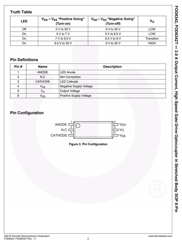
| 引脚 | 符号 | 名称 |
|---|---|---|
| 3 | A | |
| 4 | VSS | |
| 5 | VO | |
| 6 | VDD | |
| 7 | V |
数据来源:原厂规格书引脚图
关键参数速览
- 正向电流 IF
- 4. Functional operation under
- 电源电压 VCC
- -0.5 to 35
- 工作温度 TA
- -40 to +100
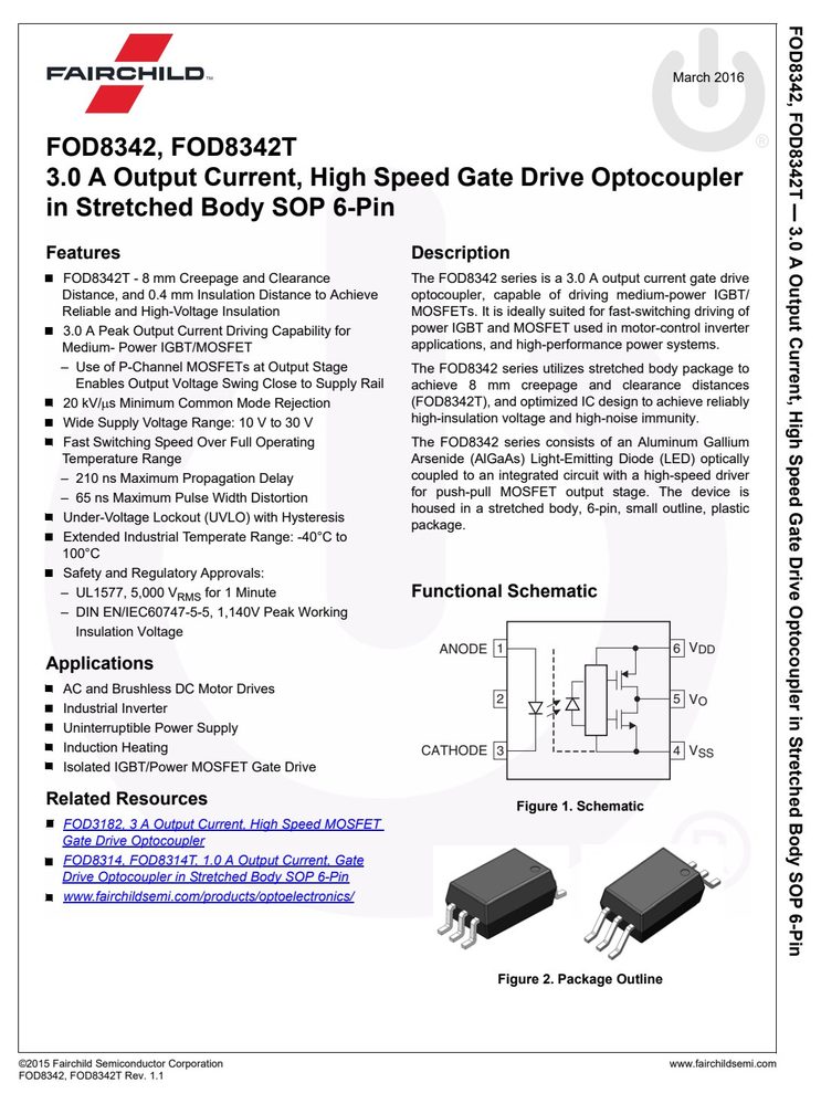
产品特点 Features
- FOD8342T - 8 mm Creepage and Clearance The FOD8342 series is a 3.0 A output current gate drive Output
- Distance, and 0.4 mm Insulation Distance to Achieve optocoupler, capable of driving medium-power IGBT/
- Reliable and High-Voltage Insulation MOSFETs. It is ideally suited for fast-switching driving of
- 3.0 A Peak Output Current Driving Capability for power IGBT and MOSFET used in motor-control inverter
- Medium- Power IGBT/MOSFET applications, and high-performance power systems. Current,
- Use of P-Channel MOSFETs at Output Stage The FOD8342 series utilizes stretched body package to
- Enables Output Voltage Swing Close to Supply Rail achieve 8 mm creepage and clearance distances
- 20 kV/s Minimum Common Mode Rejection (FOD8342T), and optimized IC design to achieve reliably
- FOD8342,
绝对最大额定值 Absolute Maximum Ratings(TA = 25°C)
超过下表数值可能造成器件永久损坏,设计时请留余量。
| 符号 | 参数 | 值 | 单位 |
|---|---|---|---|
| T Storage | Temperature | -40 to +125 | °C |
| T OPR Operating | Temperature | -40 to +100 | °C — |
| T J Junction | Temperature | -40 to +125 | °C 3.0 |
| Lead Solder | Temperature | ||
| T | 260 for 10 sec | °C A | |
| SOL (Refer to | Reflow Temperature Profile) | ||
| I Average | Input Current | 25 | mA |
| I Peak | Output Current(1) | 3 | A |
| V Supply | Voltage | -0.5 to 35 | V |
| V Peak | Output Voltage | 0 to V | V |
| PD Input Power | Dissipation(2)(4) | 45 | mW |
| PD Output | Power Dissipation(3)(4) | 500 | mW |
数据来源:原厂规格书
安全与绝缘额定值(DIN EN/IEC 60747−5−5)
| 符号 | 参数 | 值 | 单位 |
|---|---|---|---|
| FOD8342, |
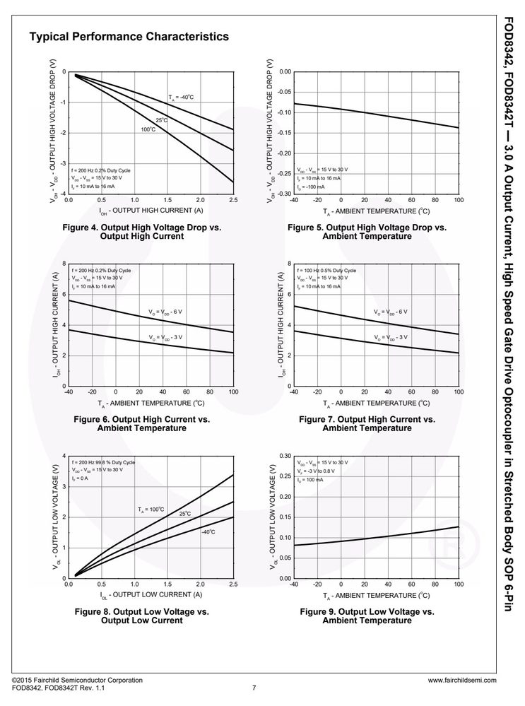
特性曲线(Typical Performance Curves)