
产品应用与封装尺寸
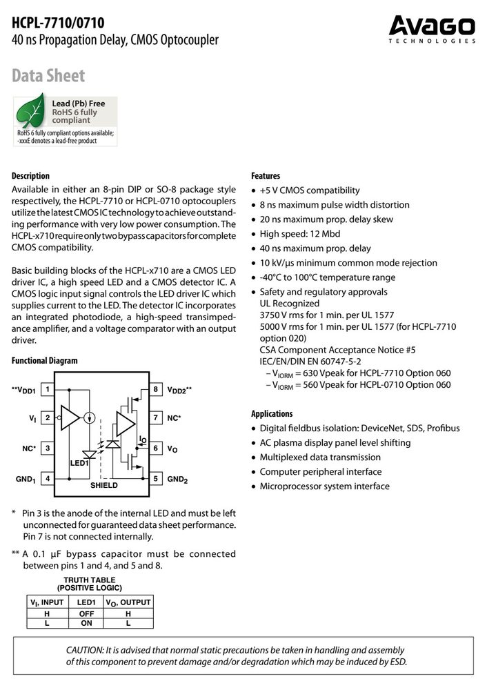
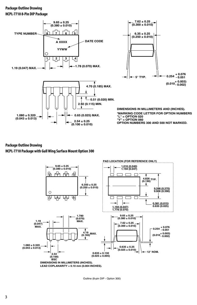
图纸取自原厂规格书,点击可放大查看原始尺寸标注。
引脚定义与内部结构
| 引脚 | 符号 | 名称 |
|---|---|---|
| 5 | GND | |
| 6 | V | |
| 7 | NC | |
| 8 | V |
数据来源:原厂规格书引脚图
关键参数速览
- 隔离电压 VISO
- for 1
- 电源电压 VCC
- 6.0
- 工作温度 TA
- VDD1 (V)
- 传输速率
- 3. Mimimum Pulse Width is the
产品特点 Features
- Available in either an 8-pin DIP or SO-8 package style • +5 V CMOS compatibility respectively, the HCPL-7710 or HCPL-0710 optocouplers
- 8 ns maximum pulse width distortion
- 20 ns maximum prop. delay skew ing performance with very low power consumption. The
- HCPL-x710 require only two bypass capacitors for complete • High speed: 12 Mbd
- CMOS compatibility. • 40 ns maximum prop. delay
- 10 kV/µs minimum common mode rejection
- Basic building blocks of the HCPL-x710 are a CMOS LED
- -40°C to 100°C temperature range driver IC, a high speed LED and a CMOS detector IC. A
- CSA Component Acceptance Notice #5
- Functional Diagram IEC/EN/DIN EN 60747-5-2
- V = 630 Vpeak for HCPL-7710 Option 060
- TRUTH TAIOBRMLE
- (POSIT I–V EV LOG I=C )560 Vpeak for HCPL-0710 Option 060
- **V 1 8 V ** IORM
- DD1 DD2
- V , INPUT LED1 V , OUTPUT
绝对最大额定值 Absolute Maximum Ratings(TA = 25°C)
超过下表数值可能造成器件永久损坏,设计时请留余量。
| 参数 | 符号 | 最小 | 最大 | 单位 |
|---|---|---|---|---|
| Storage Temperature | T | –55 | 125 | °C |
| Ambient Operating Temperature | T | –40 | +100 | °C |
| Supply Voltages | V , V DD1 DD2 | 0 | 6.0 | Volts |
| Input Voltage | V I | –0.5 | V +0.5 DD1 | Volts |
| Output Voltage | V O | –0.5 | V +0.5 DD2 | Volts |
| Input Current | I | –10 | +10 | mA |
| Average Output Current | I | 10 | mA | |
| Lead Solder Temperature | 260°C for | 10 sec., 1.6 mm | below seating | plane |
| Solder Reflow Temperature Profile | See Solder | Reflow Temperature | Profile | Section |
数据来源:原厂规格书
安全与绝缘额定值(DIN EN/IEC 60747−5−5)
| 单位 | 条件 |
|---|---|
| Minimum External Air L(I01) 7.1 4.9 | |
| Minimum External L(I02) 7.4 4.8 | |
| Minimum Internal Plastic 0.08 0.08 | |
| Tracking Resistance CTI ≥175 | |
| mm | Measured from input terminals to output |
| mm | Measured from input terminals to output |
| mm | Insulation thickness between emitter and |
| Volts | DIN IEC 112/VDE 0303 Part 1 |
| Material Group (DIN VDE 0110, 1/89, Table 1) | |
| surface of | a printed circuit board between the solder fillets |
| of the | input and output leads must be considered. There |
| are | recommended techniques such as grooves and ribs |
| which may | be used on a printed circuit board to achieve |
| Tracking Resistance CTI ≥175 | |
| Volts | DIN IEC 112/VDE 0303 Part 1 |
| Material Group (DIN VDE 0110, 1/89, Table 1) | |
| surface of | a printed circuit board between the solder fillets |
| of the | input and output leads must be considered. There |
| are | recommended techniques such as grooves and ribs |
| which may | be used on a printed circuit board to achieve |
| desired | creepage and clearances. Creepage and clearance |
| distances | will also change depending on factors such as |
| pollution 4 0 | degree and insulation level. 15 12 |
| Figure 4. Typical pulse width distortion vs. tempera- | Figure 5. Typical rise time vs. temperature. |
| HCPL-0710 fig 4 29 )sn( TPLH 15 | HCPL-0710 fig 5 6 4 2 0 |
| 15 20 25 30 35 40 45 50 | 15 20 25 30 35 40 45 50 |
| CI (pF) | CI (pF) |
| Figure 7. Typical propagation delays vs. output load | Figure 8. Typical pulse width distortion vs. output load |
| capacitance. | capacitance. |
| 10 7 6 LLAF 4 3 2 1 | STANDARD 8 PIN DIP PRODUCT 600 TUPNI 500 P REWOP 200 TUPTUO 100 |
| 0 5 10 15 20 25 30 35 | 0 |
| - TNERRUC 700 | IS (mA) |
电气特性 Electrical Characteristics(TA = 25°C)
| 参数 | 符号 | 最小 | 典型 | 最大 | 单位 | 测试条件 |
|---|---|---|---|---|---|---|
| Logic Low Input | I DD1L | 6.0 | 10.0 | mA | V = 0 V I | |
| Logic High Input | I DD1H | 1.5 | 3.0 | mA | V = V I DDI | |
| Input Supply Current | I | 13.0 | mA | |||
| Output Supply Current | I | 5.5 | 11.0 | mA | ||
| Input Current | I | -10 | 10 | µA | ||
| Logic High Output | V OH | 4.4 | 5.0 | V | I = -20 µA, V = V O I IH | |
| Voltage | 4.0 | 4.8 | I = -4 mA, V = V | |||
| Logic Low Output | V OL | 0 | 0.1 | V | I = -20 µA, V = V O I IL | |
| Voltage | 0.5 | 1.0 | I = -4 mA, V = V | |||
| Input-Output Momentary | 0710 V | 3750 | Vrms | RH = 50%, | ||
| Withstand Voltage [8, 9, 10] | t = 1 min., T = 25°C | |||||
| Resistance | R | 1012 | W | V = 500 Vdc | ||
| Capacitance | C | 0.6 | pF | f = 1 MHz | ||
| Input IC Junction-to-Case | -7710 q | 145 | °C/W | Thermocouple | ||
| Thermal Resistance | located at center | |||||
| Package Power Dissipation | P | 150 | mW | |||
| PHL | I | O | ||||
| PLH | I | O | ||||
| H | O | DD2 | L | |||
| 5 | 0 °C | 29 | ||||
| 0 °C | 85 °C | 27 | ||||
| 85 °C | 2.0 | )sn( | 25 | |||
| )V( 3 | )V( | LHP | 23 | |||
| V 2 | V | , HLP | 21 | TPHL | ||
| 0 | 1.6 | 15 | ||||
| 0 1 2 3 4 | 5 4.5 4.75 | 5 | 5.25 | 5.5 | 0 10 | 20 30 40 50 60 70 80 |
| VI (V) | VDD1 (V) | TA (C) | ||||
| HCPL-0710 fig 1 | HCPL-0710 fig | 2 | HCPL-0710 fig 3 |
相关 / 可替代型号
以上型号来自规格书与型号命名比对,参数需以各自规格书为准;下单前请与销售确认封装与脚位。
订货信息与供货形式
| 型号 | RoHS | Non | RoHS2 | Surface | Gull | 包装 | Vrms/ | 1 | IEC/EN/DIN |
|---|---|---|---|---|---|---|---|---|---|
| HCPL-0710 | and HCPL-7710 | are UL Recognized | with 3750 | Vrms for | 1 minute | per UL1577. | |||
| Part | RoHS | Non | RoHS | Surface | Gull | Tape | Vrms/ | 1 | IEC/EN/DIN |
| number | Compliant | Compliant Package | Mount | Wing | & Reel | Minute | rating | EN 60747-5-2 Quantity | |
| HCPL-7710 | -320E | -320 | X | X | X | 50 per tube | |||
| RoHS | compliant option | will | use ‘-XXXE‘. |