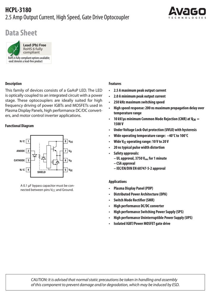
This family of devices consists of a GaAsP LED. The LED • 2.5 A maximum peak output current is optically coupled to an integrated circuit with a power • 2.0 A minimum peak output current stage. These
The HCPL-3180 contains an under voltage lockout (UVLO)
The HCPL-3180 includes a Propagation Delay Difference conditions which cause the HCPL-3180 supply voltage
(equivalent to the fully charged IGBT gate voltage) to drop below a level necessary to keep the IGBT in a low resistance state. When the HCPL-3180 output is in the high state and the supply voltage drops below the HCPL-
3180 V threshold (typ 7.5 V) the optocoupler output
UVLO- will go into the low state. When the HCPL-3180 output is in the low state and the supply voltage rises above the
HCPL-3180 V threshold (typ 8.5 V) the optocoupler
UVLO+ output will go into the high state (assume LED is “ON”).
EGATLOV 14
TUPTUO
V O 4
0 5 10 15 20
To minimize dead time in a given design, the turn on of
LED2 should be delayed (relative to the turn off of LED1) so that under worst-case conditions, transistor Q1 has just turned off when transistor Q2 turns on, as shown in
Figure 34. The amount of delay necessary to achieve this condition is equal to the maximum value of the propa- gation delay difference specification, PDD , which is
MAX specified to be 90 ns over the operating temperature range of -40 °C to +100 °C.
ILED1
绝对最大额定值 Absolute Maximum Ratings(TA = 25°C)
超过下表数值可能造成器件永久损坏,设计时请留余量。
参数
符号
(<1 µs pulse width, 300 pps)
Lead Solder Temperature
260°C for 10 sec.,
Solder Reflow Temperature
Profile See Package -55 125 °C -40 125 °C 25 mA 1 5 V -0.5 25 V 0 V V 250 mW 3 295 mW 4
CLEDP 1 2 3 4 2 4 1 2 3 Q1 4 1 2 3 4
µF + VCC = 20 V 8 7 6 5 7 5 8 7 6 CLEDN 5 8 7 6 5
数据来源:原厂规格书
安全与绝缘额定值(DIN EN/IEC 60747−5−5)
参数
符号
最小
典型
最大
单位
条件
图号
备注
Input-Output Resistance
R
10[11]
Ω
V = 500 V
9
Input-Output Capacitance
C
1
pF
Freq = 1 MHz
1. Derate linearly above
+70°C free air temperature
at a rate of
0.3 mA/°C.
minimum = 2.0 A. See
Application section for
additional
details on limiting
IOL peak.
3. Derate linearly above
+70°C, free air temperature
at the rate
of 4.8 mW/°C.
电气特性 Electrical Characteristics(TA = 25°C)
参数
符号
最小
典型
最大
单位
条件
图号
备注
Over recommended
operating conditions
unless
otherwise
specified.
High Level Output
Current I
0.5
A
V = V - 4
2, 3, 17
5
2.0
A
V = V -10
2, 3, 17
2
Low Level Output
Current I
0.5
A
V = V +2.5
5, 6, 18
5
2.0
A
V = V +10
5, 6, 18
2
High Level Output
Voltage V V
-4
V
I = -100
mA 1, 3, 19
6, 7
OH
CC
O
Low Level Output
Voltage V
0.5
V
I = 100 mA
4, 6, 20
High Level Supply
Current I
3.0
6.0
mA
Output Open
7, 8
I
= 10 to 16
mA
Low Level Supply
Current I
3.0
6.0
mA
Output Open
7, 8
V
= 3.0 to
0.8 mA
Threshold Input
Current I
8.0
mA
Low to High
I = 0 mA,
9, 15, 21
Threshold Input
Voltage V
0.8
V
V > 5 V
Input Forward Voltage
V
1.2
1.5
1.8
V
I = 10 mA
16
Temperature Coefficient
of DV /DT
–1.6
mV/°C
I = 10 mA
UVLO Threshold
V
7.9
V
I = 10 mA,
V
7.4
V
V > 5 V
22, 33
UVLO Hysteresis
UVLO
0.5
V
Input Capacitance
C
60
pF V
f = 1 MHz, = 0 V
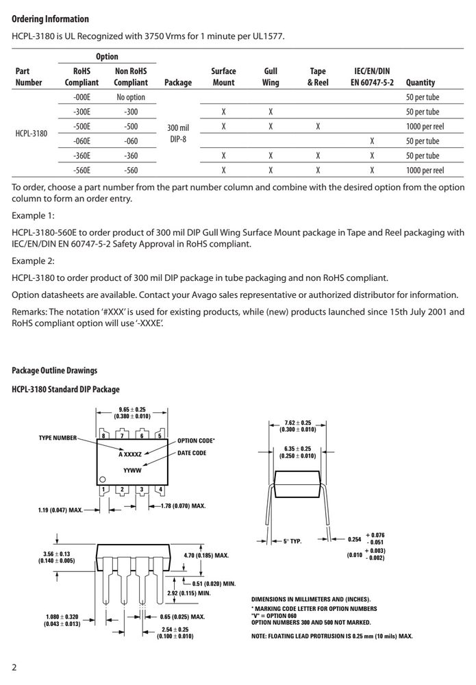
订货信息与供货形式
型号
Compliant
Compliant2
封装
Mount
Wing
&
包装
EN
60747-5-2
数量
HCPL-3180
is UL Recognized
with 3750
Vrms for
1 minute per
UL1577.
Part
RoHS
Non RoHS
Surface
Gull
Tape
IEC/EN/DIN
Number
Compliant
Compliant
Package
Mount
Wing
&
Reel
EN
60747-5-2
Quantity
应用领域 Applications
A 0.1 µF bypass capacitor must be con-Distributed Power Architecture (DPA)Switch Mode Rectifier (SMR)High performance DC/DC converterIsolated IGBT/Power MOSFET gate drive270 Ω 0.1 µF +CONTROLINPUT74XXXOPEN 4 5COLLECTORHCPL-3180 and degrade performance.