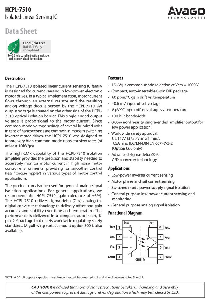
The HCPL-7510 isolated linear current sensing IC family • 15 kV/µs common-mode rejection at Vcm = 1000 V Installation classification per DIN EN 0110-1/1997-04, Table 1 for rated mains voltage ≤ 150 Vr
The HCPL-7510 isolated linear current sensing IC family
15 kV/µs common-mode rejection at Vcm = 1000 V
HCPL-7510 Gull Wing Surface Mount Option 300 Outline Drawing
Land Pattern Recommendation
9.80 ± 0.25
(0.386 ± 0.010) 1.016 (0.040)
8 7 6 5
A 7510
6.350 ± 0.25
(0.250 ± 0.010) 10.9 (0.430)
1 2 3 4
1.27 (0.050) 2.0 (0.080)
1.780 9.65 ± 0.25
(0.070) (0.380 ± 0.010)
1.19 MAX.
7.62 ± 0.25
绝对最大额定值 Absolute Maximum Ratings(TA = 25°C)
超过下表数值可能造成器件永久损坏,设计时请留余量。
参数
符号
最小
最大
单位
备注
Storage Temperature
TS
–55
125
°C
Operating Temperature
TA
–40
100
°C
Supply Voltage
VDD1, VDD2
0
6
V
Steady-State Input Voltage
VIN+, VIN-
–2.0
VDD1 + 0.5
V
Two Second Transient Input
Voltage VIN+, VIN-
–6.0
VDD1 + 0.5
V
Output Voltage
VOUT
–0.5
VDD2 + 0.5
V
Reference Input Voltage
VREF
0.0
VDD2 + 0.5
V
Reference Input Current
IREF
20
mA
Lead Solder Temperature
260°C for 10 sec.,
1.6 mm below seating
plane
数据来源:原厂规格书
安全与绝缘额定值(DIN EN/IEC 60747−5−5)
Safety-limiting
值
–
maximum
值2
allowed
in
the
event
of
a
failure.
Input to Output
Test
Voltage,
Method b[2]
Input to Output
Test
Voltage,
Method a[2]
Highest
Allowable
Overvoltage
(transient
overvoltage
tini
= 10
sec)
VIOTM 6000 Vpeak
Case
Temperature
TS 175 °C
Input
Current[3]
IS, INPUT 400 mA
Output
Power[3]
PS, OUTPUT 600 mW S 800
is Class A in
accordance
with
CECC00802.
TUPNI 500
log, under
Product
Safety
Regulations
section,
charge test
profiles.
, P S – 300
3. Refer to the
following
figure
for
dependence
of PS
and IS
on
ambient
temperature. TUPTUO 100
0 25 50 75 100 125 150 175 200
电气特性 Electrical Characteristics(TA = 25°C)
参数
符号
最小
典型
最大
单位
条件
图号
备注
Input Offset Voltage
VOS
–6
–0.6
6
mV
VIN+ = 0 V
6
1
Magnitude of Input
Offset ∆Vos/∆T
8
20
µV/°C
VIN+ = 0 V
7
Gain
G
VREF/0.512
VREF/
VREF/0.512
V/V
-0.2 V < VIN+
8, 9
2
– 3%
0.512
+ 3%
< 0.2 V TA = 25°C
Magnitude of Gain
Change ∆G/∆T
60
300
ppm/°C
-0.2 V < VIN+
9
vs. Temperature
< 0.2 V
VOUT 200 mV Nonlinearity
NL200
0.06
0.55
%
-0.2 V < VIN+ < 0.2 V
10, 11
3,4
Magnitude of VOUT
200 mV |dNL200/dT|
0.0004
%/°C
-0.2 V < VIN+
11
Nonlinearity Change
< 0.2 V
VOUT 100 mV Nonlinearity
NL100
0.04
0.4
%
-0.1 V < VIN+ < 0.1 V
10, 11
3,5
Input Supply Current
IDD1
11.7
16
mA
1,2,3
Output Supply Current
IDD2
9.9
16
mA
1,2,3
Reference Voltage
Input IREF
0.26
1
mA
Input Current
IIN+
–0.6
5
µA
VIN+ = 0 V
4
Magnitude of Input
Bias |dIIN/dT|
0.45
nA/°C
Maximum Input Voltage
|VIN+|MAX
256
mV
5
Equivalent Input
Impedance RIN
700
kΩ
VOUT Output Impedance
ROUT
15
Ω
Input DC Common-Mode
CMRRIN
63
dB
7
特性曲线(Typical Performance Curves)
典型特性曲线(原厂规格书性能曲线章节)
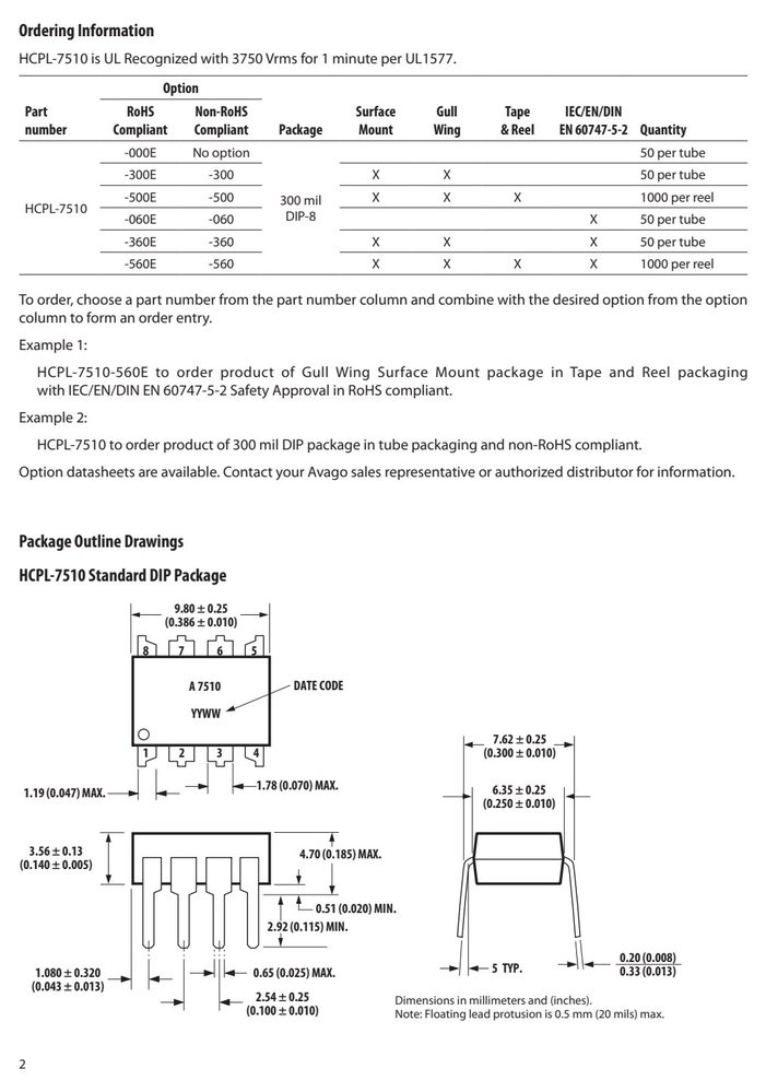
订货信息与供货形式
型号
Compliant
Compliant2
封装
Mount
Wing
&
包装
EN
60747-5-2
数量
HCPL-7510
is UL Recognized
with 3750
Vrms for 1
minute per
UL1577.
Part
RoHS
Non-RoHS
Surface
Gull
Tape
IEC/EN/DIN
number
Compliant
Compliant
Package
Mount
Wing
&
Reel
EN
60747-5-2
Quantity
with
IEC/EN/DIN EN
60747-5-2 Safety
Approval
in RoHS
compliant.
应用领域 Applications
Low-power inverter current sensingMotor phase and rail current sensingGeneral purpose analog signal isolationFunctional DiagramPower Supplies and BypassingGATE DRIVECIRCUIT5.1 VMOTOR+ R1 SENSEFLOATING