产品应用与封装尺寸
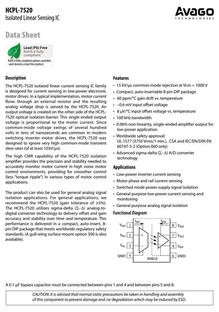
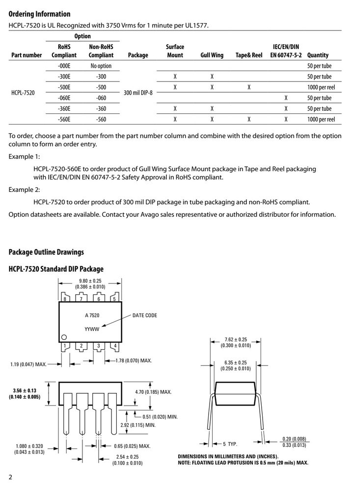
图纸取自原厂规格书,点击可放大查看原始尺寸标注。
关键参数速览
- 电源电压 VCC
- 6
- 工作温度 TA
- 100
产品特点 Features
- The HCPL-7520 isolated linear current sensing IC family
- 15 kV/µs common-mode rejection at Vcm = 1000 V
- HCPL-7520 Gull Wing Surface Mount Option 300 Outline Drawing
- 9.80 ± 0.25 Land Pattern Recommendation
- (0.386 ± 0.010)
- 1.016 (0.040)
- 8 7 6 5
- A 7520
- 6.350 ± 0.25
- YYWW (0.250 ± 0.010)
- 10.9 (0.430)
- 1 2 3 4
- 1.27 (0.050) 2.0 (0.080)
- 1.780 9.65 ± 0.25
- (0.070) (0.380 ± 0.010)
- 1.19 MAX.
绝对最大额定值 Absolute Maximum Ratings(TA = 25°C)
超过下表数值可能造成器件永久损坏,设计时请留余量。
| 参数 | 符号 | 最小 | 最大 | 单位 | 备注 |
|---|---|---|---|---|---|
| Storage Temperature | T | –55 | 125 | °C | |
| Operating Temperature | T | –40 | 100 | °C | |
| Supply Voltage | V , V | 0 | 6 | V | |
| Steady-State Input Voltage | V , V IN+ IN- | –2.0 | V + 0.5 DD1 | V | |
| Two Second Transient Input | Voltage V , V IN+ IN- | –6.0 | V + 0.5 DD1 | V | |
| Output Voltage | V OUT | –0.5 | V + 0.5 DD2 | V | |
| Reference Input Voltage | V REF | 0.0 | V + 0.5 DD2 | V | |
| Reference Input Current | I | 20 | mA | ||
| Lead Solder Temperature | 260°C for 10 sec., | 1.6 mm below | seating plane |
数据来源:原厂规格书
安全与绝缘额定值(DIN EN/IEC 60747−5−5)
| Safety-limiting | 值 | – | maximum | 值2 | allowed | in | the | event | of | a | failure. |
|---|---|---|---|---|---|---|---|---|---|---|---|
| Input to Output | Test | Voltage, | Method b[2] | ||||||||
| V x | 1.875 = V | , 100% | production | test with | t | = 1 | sec, | partial | discharge <5 pC V 1670 V | ||
| IORM | PR | m | PR peak | ||||||||
| Input to Output | Test | Voltage, | Method a[2] | ||||||||
| V x 1.5 | = V , | type | and sample | test, | t = 60 | sec, | partial | discharge | <5 pC V 1336 V | ||
| IORM | PR | m | PR peak | ||||||||
| Highest | Allowable | Overvoltage | (transient | overvoltage | t ini | = 10 | sec) | V 6000 V IOTM peak | |||
| Case | Temperature | T 175 °C | |||||||||
| Input | Current[3] | I 400 mA | |||||||||
| Output | Power[3] | P 600 mW | |||||||||
| Insulation | Resistance | at T | , V = | 500 V | R >109 Ω | ||||||
| S | IO | S | |||||||||
| 1. Insulation | characteristics | are | guaranteed | only | within | the | safety | I | S | PS (mW) | |
| maximum | ratings | which | must be | ensured by | protective | circuits | – TNERRUC | 700 | IS (mA) | ||
| within the | application. | Surface | Mount | Classifications | is | Class | A in | ||||
| 2. Refer to the | optocoupler | section of | the | Isolation and | Control | TUPNI | 500 |
电气特性 Electrical Characteristics(TA = 25°C)
| 参数 | 符号 | 最小 | 典型 | 最大 | 单位 | 条件 | 图号 | 备注 |
|---|---|---|---|---|---|---|---|---|
| IN+ | IN- | REF | ||||||
| Input Offset Voltage | V | –6 | –0.6 | 6 | mV | V = 0 V | 6 | 1 |
| Magnitude of Input | Offset ∆Vos/∆T | 8 | 20 | µV/°C | V = 0 V | 7 | ||
| Gain | G | V /0.512 | V | V /0.512 | V/V | -0.2 V < V | 8, 9 | 2 |
| REF | REF | REF | IN+ | |||||
| – 5% | /0.512 | + 5% | < 0.2 V T = 25°C | |||||
| Magnitude of Gain | Change ∆G/∆T | 60 | 300 | ppm/°C | -0.2 V < V | 9 | ||
| vs. Temperature | < 0.2 V | |||||||
| V 200 mV Nonlinearity | NL | 0.06 | 0.55 | % | -0.2 V < V | 10, | 3,4 | |
| OUT | 200 | IN+ < 0.2 V | 11 | |||||
| Magnitude of V | 200 mV |dNL /dT| | 0.0004 | %/°C | -0.2 V < V | 11 | |||
| OUT | 200 | IN+ | ||||||
| Nonlinearity Change | < 0.2 V | |||||||
| V 100 mV Nonlinearity | NL | 0.04 | 0.4 | % | -0.1 V < V | 10, | 3,5 | |
| OUT | 100 | IN+ < 0.1 V | 11 | |||||
| Input Supply Current | I | 11.7 | 16 | mA | 1,2,3 | |||
| Output Supply Current | I | 9.9 | 16 | mA | 1,2,3 | |||
| Reference Voltage | Input I | 0.26 | 1 | mA | ||||
| Input Current | I | –0.6 | 5 | µA | V = 0 V | 4 | ||
| Magnitude of Input | Bias |dI /dT| | 0.45 | nA/°C | V = 0 V | ||||
| Maximum Input | Voltage |V | | 256 | mV | 5 | ||||
| Equivalent Input | Impedance R | 700 | kΩ | |||||
| V OUT Output Impedance | R OUT | 15 | Ω | |||||
| Input DC Common-Mode | CMRR | 63 | dB | 7 |
特性曲线(Typical Performance Curves)