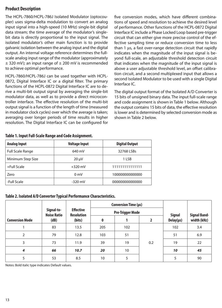
产品应用与封装尺寸
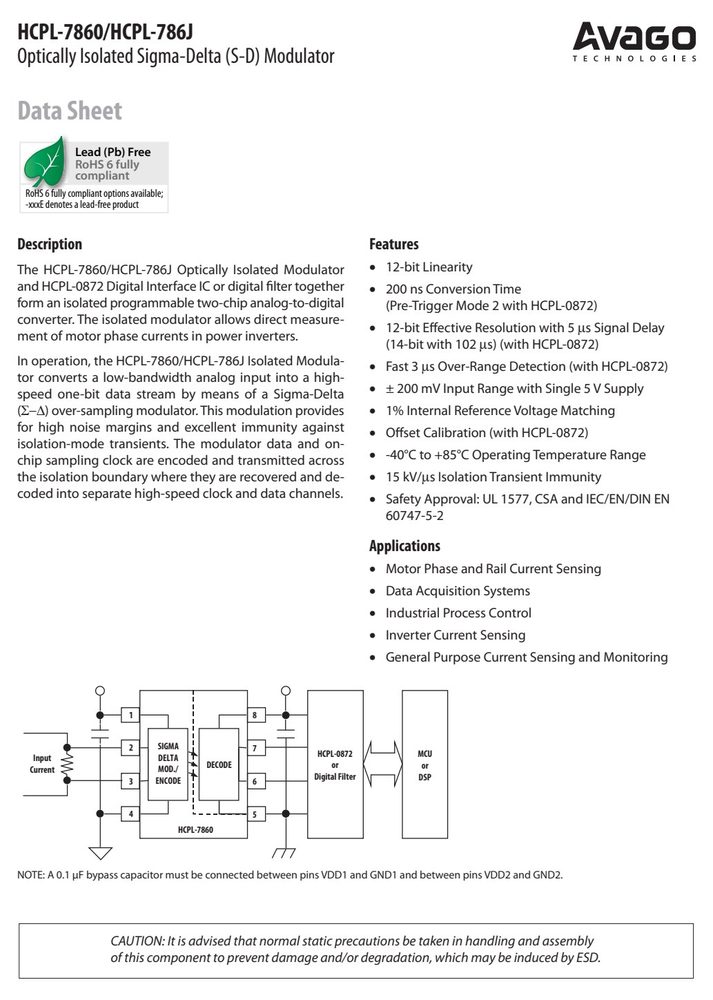
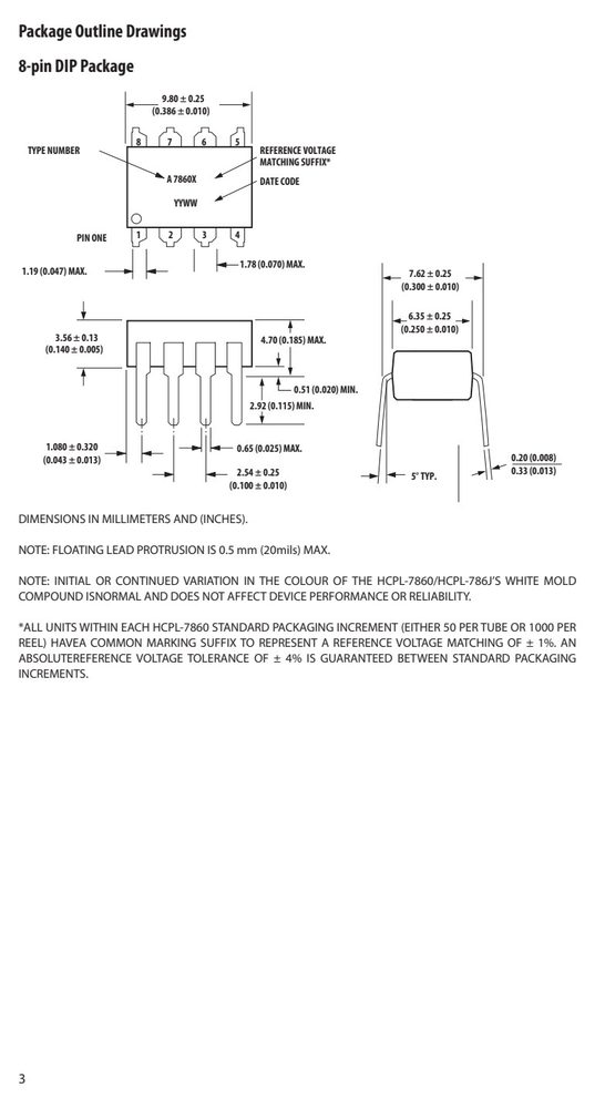
图纸取自原厂规格书,点击可放大查看原始尺寸标注。
引脚定义与内部结构
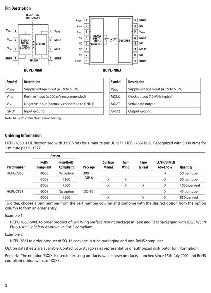
| 引脚 | 符号 | 名称 |
|---|---|---|
| 9 | 80 ± 0.25 | |
| 1 | 016 (0.040) | |
| 6 | 350 ± 0.25 | |
| 10 | 9 (0.430) | |
| 2 | 0 (0.080) | |
| 0 | 33 (0.013) | |
| 3 | 56 ± 0.13 | |
| 8 | 763 ± 0.254 |
数据来源:原厂规格书引脚图
关键参数速览
- 隔离电压 VISO
- 18
- 电源电压 VCC
- 5.5
- 工作温度 TA
- 85
产品特点 Features
- In operation, the HCPL-7860/HCPL-786J Isolated Modula- tor converts a low-bandwidth analog input into a high- speed one-bit data stream by means of a Sigma-Delta
- 12-bit Linearity
- 200 ns Conversion Time
- (Pre-Trigger Mode 2 with HCPL-0872)
- 12-bit Effective Resolution with 5 s Signal Delay
- (14-bit with 102 s) (with HCPL-0872)
- Fast 3 s Over-Range Detection (with HCPL-0872)
- ± 200 mV Input Range with Single 5 V Supply
- 1% Internal Reference Voltage Matching
- Offset Calibration (with HCPL-0872)
- -40°C to +85°C Operating Temperature Range
- 15 kV/s Isolation Transient Immunity
绝对最大额定值 Absolute Maximum Ratings(TA = 25°C)
超过下表数值可能造成器件永久损坏,设计时请留余量。
| 参数 | 符号 | 最小 | 最大 | 单位 | 备注 |
|---|---|---|---|---|---|
| Storage Temperature | T | -55 | 125 | °C | |
| Ambient Operating Temperature | T | -40 | 85 | °C | |
| Supply Voltages | V , V | 0 | 5.5 | V | |
| Steady-State Input Voltage | V , V IN+ IN- | -2.0 | V + 0.5 DD1 | V | 1 |
| Two Second Transient Input | Voltage | -6.0 | |||
| Output Voltages | MCLK, MDAT | -0.5 | V + 0.5 DD2 | V | |
| Lead Solder Temperature | 260°C for 10 | sec., 1.6 mm below | seating plane | ||
| Solder Reflow Temperature | Profile See Maximum | Solder Reflow | Thermal Profile | section |
数据来源:原厂规格书
安全与绝缘额定值(DIN EN/IEC 60747−5−5)
| Safety-limiting | 值 | - | maximum | 值2 | allowed | in | the | event | of | a | failure. |
|---|---|---|---|---|---|---|---|---|---|---|---|
| Input to Output | Test | Voltage, | Method b [2] | V 1670 2306 Vpeak | |||||||
| V x 1.875=V | , | 100% | Production | Test | with t | =1 | sec, | ||||
| Input to Output | Test | Voltage, | Method a[2] | V 1425 1968 Vpeak | |||||||
| V x 1.6=V | , Type | and | Sample | Test, t | =10 | sec, | |||||
| Highest | Allowable | Overvoltage(Transient | Overvoltage | t | = | 60 | sec) | V 6000 8000 Vpeak | |||
| Case | Temperature | T 175 175 °C | |||||||||
| Input Current | [3] | I 400 400 mA | |||||||||
| Output | Power [3] | P 600 600 mW | |||||||||
| Insulation | Resistance | at T | , V = | 500 V | R >109 >109 | ||||||
| A in accordance | with | CECC00802. | TNERRUC | ||||||||
| tion of Method | a and | Method | b | partial | discharge test | profiles. | |||||
| 3. Refer to the | following | figure | for | dependence | of P | and I | on | ambient | temperature. | ||
| S | S | - REWOP 300 TUPTUO 200 | |||||||||
| 0 25 50 75 100 125 150 175 200 | |||||||||||
| Option 300 - | surface | mount | classification | is | Class | A | in | accordance | with CECC 00802. | ||
| (Clearance) | shortest distance through air. | ||||||||||
| (Creepage) | shortest distance path along body. | ||||||||||
| Minimum | Internal | Plastic | 0.5 | 0.5 | mm | Through insulation distance conductor to conductor, | |||||
| Gap (Internal | Clearance) | usually the straight line distance thickness between | |||||||||
| Tracking | Resistance | CTI | >175 | >175 | V | DIN IEC 112/VDE 0303 Part 1 | |||||
| Isolation Group | IIIa | IIIa | Material Group (DIN VDE 0110, 1/89, Table 1) |
电气特性 Electrical Characteristics(TA = 25°C)
| 参数 | 符号 | 最小 | 典型 | 最大 | 单位 | 条件 | 图号 | 备注 |
|---|---|---|---|---|---|---|---|---|
| DD1 DD2 | IN+ | IN- | A A | |||||
| Average Input Bias | Current I | -0.8 | μA | 1 | 3 | |||
| Average Input Resistance | R | 450 | k | 3 | ||||
| Input DC Common-Mode | CMRR | 60 | dB | 4 | ||||
| Output Logic High | Voltage V | 3.9 | 4.9 | V | I = -100 μA | |||
| Output Logic Low | Voltage V | 0.1 | 0.6 | V | I = 1.6 mA | |||
| Output Short Circuit | Current |I | OSC | 30 | mA | V = V OUT DD2 or GND2 | 5 | |||
| Input Supply Current | I DD1 | 10 | 15 | mA | V = -350 mV IN+ to +350 mV | 2 | ||
| Output Supply Current | I | 10 | 15 | mA | 3 | |||
| Output Clock Frequency | f | 8.2 | 10 | 13.2 | MHz | 4 | ||
| Data Hold Time | t | 15 | ns | 6 | ||||
| A DD1 | DD2 | A | ||||||
| Resolution | 15 | bits | 7 | |||||
| Integral Nonlinearity | INL | 3 | 30 | LSB | 5 | 8 | ||
| 0.01 | 0.14 | % | 6 | 8 | ||||
| Differential Nonlinearity | DNL | 1 | LSB | 9 | ||||
| Uncalibrated Input Offset | V | -3 | 0 | 3 | mV | V = 0 V | 7 | |
| Offset Drift vs. Temperature | dV /dT | 2 | 10 | μV/°C | V = 0 V | 7 | 10 | |
| Offset drift vs. VDD1 | dV /dV OS DD1 | 0.12 | mV/V | V = 0 V IN+ | 7 | |||
| Internal Reference Voltage | V | 320 | mV | 8 | ||||
| Absolute Reference Voltage | Tolerance | -4 | 4 | % | 8 | 2 | ||
| Reference Voltage | HCPL-7860 | -1 | 1 | % | T = 25°C. | 8 | 2 | |
| HCPL-786J | -2 | 2 | % | |||||
| V Drift vs. Temperature | dV /dT | 60 | ppm/°C. | 8 | ||||
| V Drift vs. VDD1 | dV /dV | 0.2 | % | 8 | ||||
| Full Scale Input Range | -V | +V | mV | 11 | ||||
| Recommended Input | Voltage Range | -200 | +200 | mV | ||||
| DYNAMIC CHARACTERISTICS | (Digital Interface IC | HCPL-0872 is set | to Conversion | Mode | 3.) | |||
| Signal-to-Noise Ratio | SNR 62 | 73 | dB | V 400 | = 35 Hz, mV | 9,10 | ||
| Total Harmonic Distortion | THD | -67 | dB | (141 | mV ) | |||
| Signal-to-(Noise + Distortion) | SND | 66 | dB | sine | wave. | |||
| Effective Number of Bits | ENOB 10 | 12 | bits | 11 | 12 | |||
| Conversion Time | t | 0.2 | 0.8 | μs | Pre-Trigger Mode | 2 1,12 | 13 | |
| t | 19 | 23 | μs | Pre-Trigger Mode | 1 1,12 | 13 | ||
| t | 39 | 47 | μs | Pre-Trigger Mode | 0 1,12 | |||
| Signal Delay | t | 19 | 23 | μs | 13 | 14 | ||
| Over-Range Detect Time | t 2.0 OVR1 | 3.0 | 4.2 | μs | V IN+ step | = 0 to 400mV waveform | 14 | 15 |
| Threshold Detect Time | (default t | 10 | μs | 16 | ||||
| Signal Bandwidth | BW 18 | 22 | kHz | 15 | 17 | |||
| Isolation Transient Immunity | CMR 15 | 20 | kV/μs V | = 1 kV | 18 | |||
| Input-Output | Momentary V | HCPL-7860 | 3750 | Vrms | RH ≤ 50%, t = 1 | min; 19, 20 |
特性曲线(Typical Performance Curves)