产品应用与封装尺寸
图纸取自原厂规格书,点击可放大查看原始尺寸标注。
引脚定义与内部结构
| 引脚 | 符号 | 名称 |
|---|---|---|
| 4 | 150 | |
| 5 | GND | |
| 6 | A | |
| 7 | B | |
| 8 | V |
数据来源:原厂规格书引脚图
产品特点 Features
- Bidirectional Transceivers
- Meet or Exceed the Requirements of ANSI
- Standards TIA/EIA-422-B and TIA/EIA-485-A and ITU Recommendations V.11 and X.27
- Designed for Multipoint Transmission on
- Long Bus Lines in Noisy Environments
- 3-State Driver and Receiver Outputs
- Individual Driver and Receiver Enables
- Wide Positive and Negative Input/Output
- Voltage Ranges
- ± 60-mA Max Driver Output Capability
- Thermal Shutdown Protection
- Driver Positive and Negative Current
- 12-kΩ Min Receiver Input Impedance
- ± 200-mV Receiver Input Sensitivity
- TIA/EIA-422-B and TIA/EIA-485-A and ITU
- Recommendations V.11 and X.27.
绝对最大额定值 Absolute Maximum Ratings(TA = 25°C)
超过下表数值可能造成器件永久损坏,设计时请留余量。
| 最小 | 最大 | 单位 |
|---|---|---|
| over operating free-air temperature range (unless otherwise noted)(1) | ||
| V Supply voltage(2) | 7 | V |
| Voltage range at any bus terminal –10 | 15 | V |
| V Enable input voltage D package PS package | 5.5 97 95 | V |
| T Operating virtual junction temperature | 150 | °C |
| Lead temperature 1,6 mm (1/16 inch) from case for 10 seconds | 260 | °C |
| T Storage temperature range –65 | 150 | °C |
| V | V , V | V , V |
| O | oa ob | oa ob |
| |V | | V | V |
| OD1 | o | o |
| |V | | V (R = 100 Ω) | V (R = 54 Ω) |
| OD2 | t L | t L |
| ∆|V | | | |V| – |V | | | | |V – |V | | |
| V | |V | | |V | |
| OC | os | os |
| ∆|V | | |V – V | | |V – V | |
| I | |I |, |I | | I , I |
| O | xa xb | ia ib |
数据来源:原厂规格书
电气特性 Electrical Characteristics(TA = 25°C)
| 参数 | 测试条件 | 最小 | TYP(2) | 最大 | 单位 |
|---|---|---|---|---|---|
| V Input clamp voltage | I = –18 mA | –1.5 | V | ||
| V Output voltage | I = 0 | 0 | 6 | V | |
| |V | Differential output voltage | I = 0 | 1.5 | 3.6 | 6 | V |
| R = 100 Ω, see Figure 1 L | 1/2 V or 2 (3) OD1 | ||||
| R = 54 Ω, see Figure 1 | 1.5 | 2.5 | 5 | ||
| V Differential output voltage | See (4) | 1.5 | 5 | V | |
| ∆|V | | R = 54 Ω or 100 Ω, see Figure 1 | ±0.2 +3 | V | ||
| V Common-mode output voltage | R = 54 Ω or 100 Ω, see Figure 1 | V | |||
| OC | L | –1 | |||
| ∆|V | common-mode output | R = 54 Ω or 100 Ω, see Figure 1 V = 12 V | ±0.2 1 | V | ||
| I Output current | Output disabled(6) O V = –7 V | –0.8 | mA | ||
| I High-level input current | V = 2.4 V | 20 | µA | ||
| I Low-level input current | V = 0.4 V V = –7 V V = 0 | –400 –250 –150 | µA | ||
| I Short-circuit output current | V = V V = 12 V | 250 250 | mA | ||
| Outputs enabled | 42 | 70 | |||
| I Supply current (total package) | No load | mA | |||
| Outputs disabled | 26 | 35 |
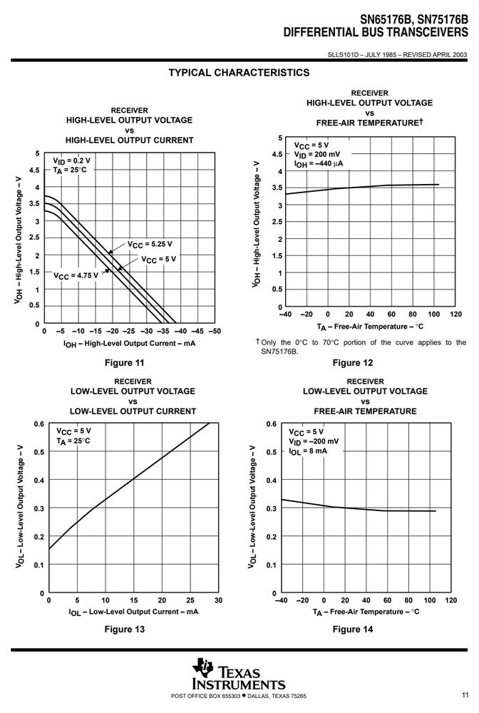
特性曲线(Typical Performance Curves)