
产品应用与封装尺寸
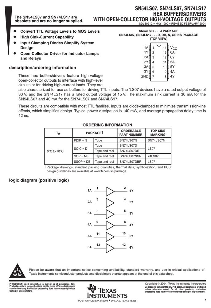
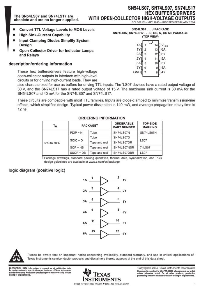
图纸取自原厂规格书,点击可放大查看原始尺寸标注。
引脚定义与内部结构
| 引脚 | 符号 | 名称 |
|---|---|---|
| 7 | V | |
| 8 | 4Y | |
| 9 | 4A | |
| 10 | 5Y | |
| 11 | 5A | |
| 12 | 6Y | |
| 13 | 6A | |
| 14 | V | |
| 15 | V |
数据来源:原厂规格书引脚图
关键参数速览
- 电源电压 VCC
- −1.5 V
产品特点 Features
- open-collector outputs to interface with high-level circuits or for driving high-current loads. They are also characterized for use as buffers for driving TTL
- 30 V, and the SN74LS17 has a rated output
- SN54LS07 and 40 mA for the SN74LS07 and
- These circuits are compatible with most TTL effects, which simplifies design. Typical power
- 12 ns.
- ORDERING
- TA PACKAGE†
- PDIP − N Tube
- SSOOIICC −− DD
- 00°CC ttoo 7700°CC Tape and
- SOP − NS Tape and
- SSOP − DB Tape and
- GND 7 8 4Y
- The ’LS07 devices have a rated output voltage of of 15 V. The maximum sink current is 30 mA for the
- Inputs are diode-clamped to minimize transmission-line is 140 mW, and average propagation delay time is
- ORDERABLE TOP-SIDE
电气特性 Electrical Characteristics(TA = 25°C)
| 最小 | 最大 | 最小2 | 最大2 |
|---|---|---|---|
| SN54LS07 | SN74LS07 | ||
| PPAARRAAMMEETTEERR TTEESSTT CCOONNDDIITTIIOONNSS‡‡ | SN74LS17 | UUNNIITT | |
| VIK VCC = MIN, II = −12 mA | −1.5 | −1.5 V | |
| ’LS07, VOH = 30 V | 0.25 | 0.25 | |
| IIOOHH VVCCCC == MMIINN,, VVIIHH == 22 VV | mmAA | ||
| SN74LS17, VOH = 15 V | 0.25 | ||
| IOL = 16 mA | 0.4 | 0.4 | |
| VVOOLL VVCCCC == MMIINN,, VVIILL == 00..88 VV | VV | ||
| IOL = MAX§ | 0.7 | 0.7 | |
| II VCC = MAX, VI = 7 V | 1 | 1 mA | |
| IIH VCC = MAX, VI = 2.4 V | 20 | 20 µA | |
| IIL VCC = MAX, VI = 0.4 V | −0.2 | −0.2 mA | |
| ICCH VCC = MAX | 14 | 14 mA | |
| ICCL VCC = MAX | 45 | 45 mA | |
| switching characteristics, V = 5 V, T = 25°C (see Figure 1) | |||
| PPAARRAAMMEETTEERR TTEESSTT CCOONNDDIITTIIOONNSS | MMIINN | TTYYPP | MMAAXX UUNNIITT |
| tPLH | 6 | 10 | |
| AA YY RRLL == 111100 ΩΩ,, CCLL == 1155 ppFF | nnss | ||
| tPHL | 19 | 30 | |
| POST OFFICE BOX 655303 DALLAS, TEXAS 75265 | 3 |