产品应用与封装尺寸
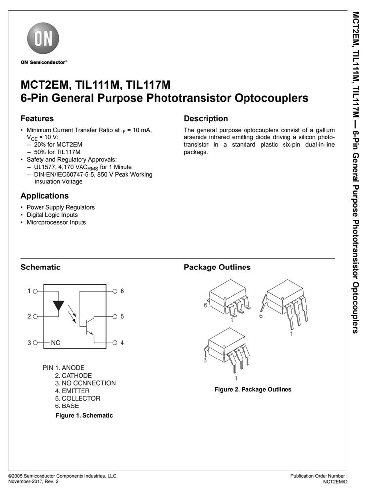
图纸取自原厂规格书,点击可放大查看原始尺寸标注。
引脚定义与内部结构
| 引脚 | 符号 | 名称 |
|---|---|---|
| 6 | V | |
| 7 | V | |
| 8 | T | |
| 9 | R | |
| 10 | V |
数据来源:原厂规格书引脚图
关键参数速览
- 正向电压 VF
- 1.50
- 正向电流 IF
- 3
- 工作温度 TA
- -40 to +100
产品特点 Features
- Minimum Current Transfer Ratio at I = 10 mA, The general purpose optocouplers consist of a gallium
- F 6-Pin
- V = 10 V: arsenide infrared emitting diode driving a silicon photo-
- 20% for MCT2EM transistor in a standard plastic six-pin dual-in-line
- 50% for TIL117M package.
- General
- Safety and Regulatory Approvals:
- UL1577, 4,170 VAC for 1 Minute
- DIN-EN/IEC60747-5-5, 850 V Peak Working
- MCT2EM,
绝对最大额定值 Absolute Maximum Ratings(TA = 25°C)
超过下表数值可能造成器件永久损坏,设计时请留余量。
| 符号 | 参数 | 器件 | 值 | 单位 |
|---|---|---|---|---|
| TIL117M | ||||
| T Storage | Temperature | All | -40 to +125 | °C |
| T Operating | Temperature | All | -40 to +100 | °C |
| T Junction | Temperature | All | -40 to +125 | ºC |
| T Lead Solder | Temperature | All | 260 for 10 seconds | °C — |
| Total Device | Power Dissipation @ T = 25°C | All | 250 | mW 6-Pin |
| Derate | Above 25°C | All | 2.94 | mW/°C |
| I DC/Average | Forward Input Current | All | 60 | mA |
| TIL111M | 3 | V | ||
| MCT2EM, TIL117M | 6 | V | ||
| I (pk) Forward | Current – Peak (300 µs, 2% Duty | Cycle) All | 3 | A |
| LED Power | Dissipation @ T = 25°C | All | 120 | mW |
| Derate | Above 25°C | All | 1.41 | mW/°C |
| V | Collector-to-Emitter Voltage | All | 30 | V |
| V Collector-to-Base | Voltage | All | 70 | V |
| V | Emitter-to-Collector Voltage | All | 7 | V |
| V Emitter-to-Base | Voltage | All | 7 | V |
| Detector | Power Dissipation @ T = 25°C | All | 150 | mW |
| Derate | Above 25°C | All | 1.76 | mW/°C Optocouplers |
数据来源:原厂规格书
安全与绝缘额定值(DIN EN/IEC 60747−5−5)
| 符号 | 参数 | 值 | 单位 | 6-Pin |
|---|---|---|---|---|
| MCT2EM, TIL111M, | ||||
| Installation Classifications | per DIN VDE < 150 V RMS | I–IV | ||
| 0110/1.89 Table 1, For Rated | Mains Voltage < 300 V | I–IV | ||
| Climatic Classification | 55/100/21 | TIL117M | ||
| Pollution Degree (DIN VDE | 0110/1.89) | 2 | ||
| Comparative Tracking Index | 175 | |||
| Input-to-Output | Test Voltage, Method A, V x 1.6 = V | , | ||
| IORM | PR 1360 | V | ||
| Type and | Sample Test with t = 10 s, Partial Discharge < | 5 pC | peak | |
| Input-to-Output | Test Voltage, Method B, V x 1.875 = | V , | ||
| IORM | PR 1594 | V | ||
| 100% Production | Test with t = 1 s, Partial Discharge < 5 | pC | peak | |
| V Highest Allowable | Over-Voltage | 6000 | V | Purpose |
| External | Creepage | ≥ 7 | mm | |
| External | Clearance | ≥ 7 | mm | |
| External | Clearance (for Option TV, 0.4" Lead Spacing) | ≥ 10 | mm | |
| T Case Temperature(1) | 175 | °C | ||
| I Input Current(1) | 350 | mA | ||
| P Output Power(1) | 800 | mW | ||
| R Insulation | Resistance at T , V = 500 V(1) | > 109 | Ω | MCT2EM, |
电气特性 Electrical Characteristics(TA = 25°C)
| 符号 | 参数 | 测试条件 | 最小 | 典型 | 最大 | 单位 |
|---|---|---|---|---|---|---|
| TIL111M, | ||||||
| V Input | Forward Voltage | I = 10 mA | 1.18 | 1.50 | V | |
| BV | Collector-to-Emitter Breakdown | Voltage I = 1.0 mA, I = 0 | 30 | 100 | V | |
| BV | Collector-to-Base Breakdown | Voltage I = 100 µA, I = 0 | 70 | 120 | V | |
| CBO | C F | — | ||||
| BV | Emitter-to-Base Breakdown Voltage | I = 10 uA, I = 0 | 7 | 10 | V | |
| EBO | E F | 6-Pin | ||||
| BV | Emitter-to-Collector Breakdown | Voltage I = 100 µA, I = 0 | 7 | 10 | V | |
| I | Collector-to-Emitter Dark Current | V = 10 V, I = 0 | 1 | 50 | nA | |
| I | Collector-to-Base Dark Current | V = 10 V | 20 | nA | ||
| C | Capacitance | V = 0 V, f = 1 MHz | 8 | pF | ||
| Transfer Characteristics | Purpose |
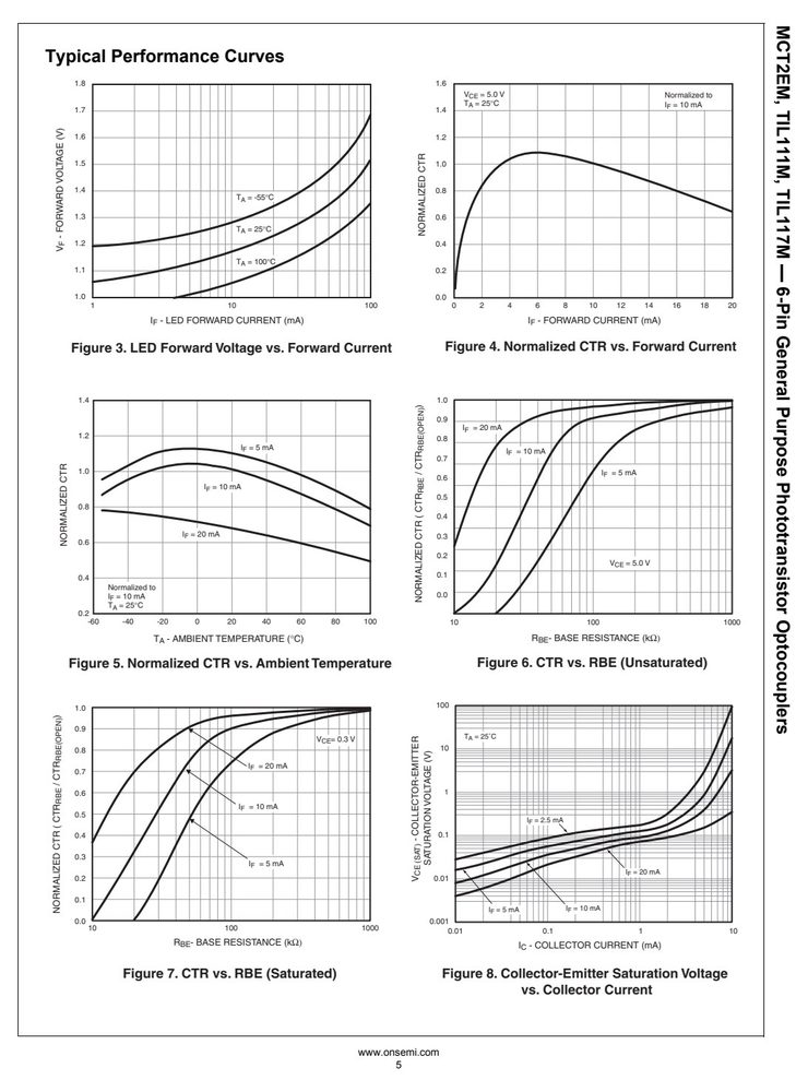
特性曲线(Typical Performance Curves)