
引脚定义与内部结构
| 引脚 | 符号 | 名称 |
|---|---|---|
| 5 | V | |
| 6 | CANL | |
| 7 | CANH | |
| 8 | MODE |
数据来源:原厂规格书引脚图
产品特点 Features
- 2.1 General n Fully ISO 11898-2 compliant n Suitable for 12 V and 24 V systems
- 6.2.1 TXD dominant time-out function
- A ‘TXD dominant time-out’ timer is started when pin TXD is set LOW. If the LOW state on pin TXD persists for longer than t , the transmitter is disabled, releasing the bus to(dom)TXD
- TJA1051
- High-speed CAN transceiver failure from driving the bus lines to a permanent dominant state (blocking all network communications). The TXD dominant time-out timer is reset when pin TXD is set HIGH.
- The TXD dominant time-out time also defines the minimum possible bit rate of 40 kbit/s.
- 6.2.2 Internal biasing of TXD and S input pins
- Pin TXD has an internal pull-up to V and pin S has an internal pull-down to GND. This ensures a safe, defined state in case one or both of these pins are left floating.
- 6.2.3 Undervoltage detection on pins V and V
- CC IO
- Should V or V drop below their respective undervoltage detection levels (V
- CC IO uvd(VCC) and V ; see Table 6), the transceiver will switch off and disengage from the bus uvd (VIO)
- (zero load) until V and V have recovered.
- 6.2.4 Over-temperature protection
- 6.3 V supply pin
- Two versions of the TJA1051 are available, only differing in the function of a single pin. Pin
绝对最大额定值 Absolute Maximum Ratings(TA = 25°C)
超过下表数值可能造成器件永久损坏,设计时请留余量。
| 符号 | 参数 | 条件 |
|---|---|---|
| V | voltage on pin x | no time limit; DC value - 58 +58 V - 0.3 +7 V |
| [1] - 150 +100 V [2] |
数据来源:原厂规格书
应用领域 Applications
产品应用与封装尺寸
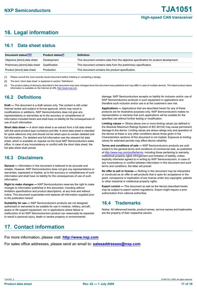
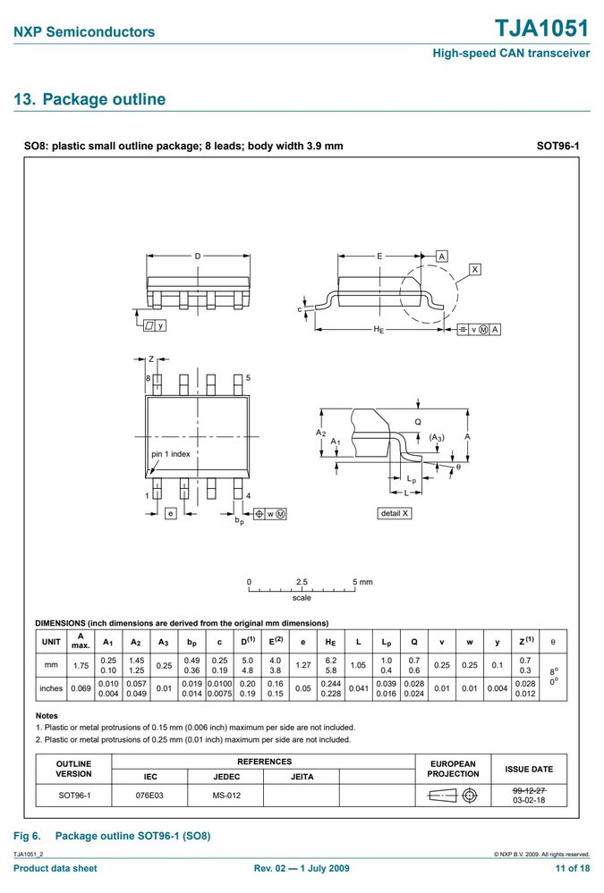
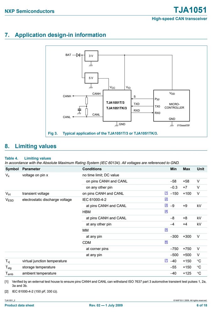
图纸取自该型号原厂规格书的应用电路与封装尺寸章节,点击图片可放大查看原始尺寸标注。