产品应用与封装尺寸
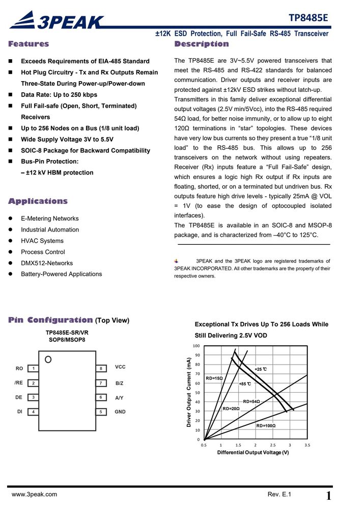
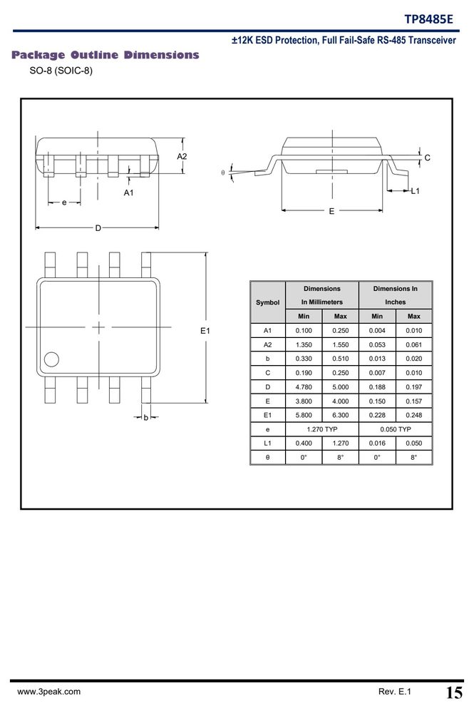
图纸取自原厂规格书,点击可放大查看原始尺寸标注。
引脚定义与内部结构
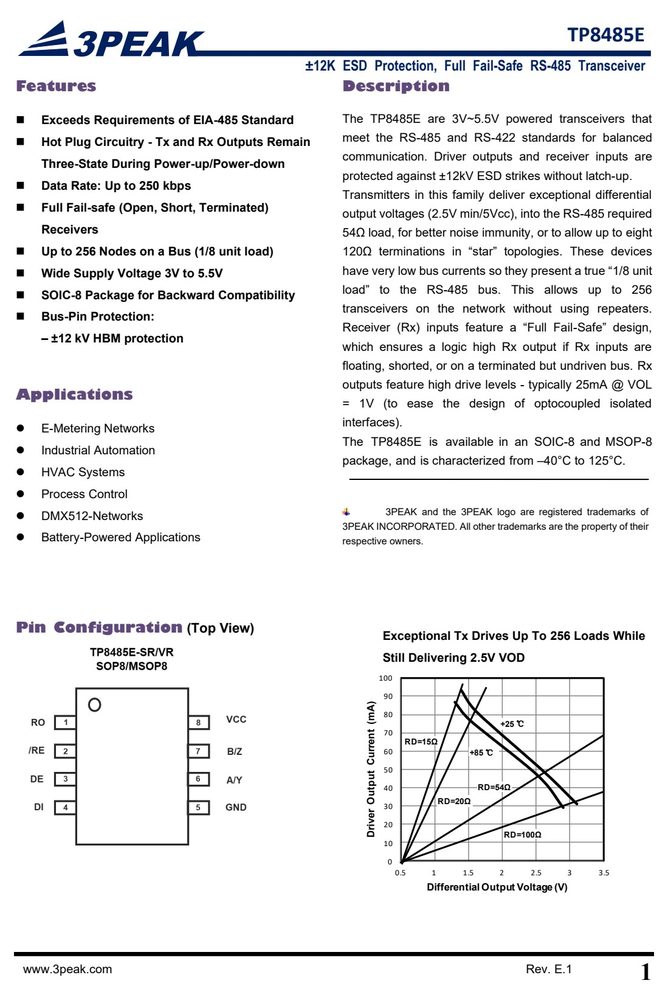
| 引脚 | 符号 | 名称 |
|---|---|---|
| 1 | RO | |
| 2 | V | |
| 3 | DE | |
| 4 | DI | |
| 5 | GND | |
| 6 | A/Y | |
| 7 | B/Z | |
| 8 | VCC |
数据来源:原厂规格书引脚图
产品特点 Features
- ◼ Exceeds Requirements of EIA-485 Standard The TP8485E are 3V~5.5V powered transceivers that meet the RS-485 and RS-422 standards for balanced
- ◼ Hot Plug Circuitry - Tx and Rx Outputs Remain communication. Driver outputs and receiver inputs are
- Three-State During Power-up/Power-down protected against ±12kV ESD strikes without latch-up.
- ◼ Data Rate: Up to 250 kbps
- Transmitters in this family deliver exceptional differential
- ◼ Full Fail-safe (Open, Short, Terminated) output voltages (2.5V min/5Vcc), into the RS-485 required
- Receivers
- 54Ω load, for better noise immunity, or to allow up to eight
- ◼ Up to 256 Nodes on a Bus (1/8 unit load) 120Ω terminations in “star” topologies. These devices
- ◼ Wide Supply Voltage 3V to 5.5V have very low bus currents so they present a true “1/8 unit load” to the RS-485 bus. This allows up to 256
- ◼ SOIC-8 Package for Backward Compatibility transceivers on the network without using repeaters.
- ◼ Bus-Pin Protection:
- Receiver (Rx) inputs feature a “Full Fail-Safe” design,
- ±12 kV HBM protection which ensures a logic high Rx output if Rx inputs are floating, shorted, or on a terminated but undriven bus. Rx
- TP8485E utilize a differential input receiver for maximum noise immunity and common mode rejection. Input sensitivity is better than
- 4kΩ, and is eight times the RS-485 “Unit Load (UL)” requirement of 12kΩ minimum. Thus, these products are known as “one-eighth
绝对最大额定值 Absolute Maximum Ratings(TA = 25°C)
超过下表数值可能造成器件永久损坏,设计时请留余量。
| Recommended | Operating | 条件 | 备注 | 2 |
|---|---|---|---|---|
| DI, DE, | RE………………………………………………………………………….…………………….....-0.3V | to (VCC + 0.3V) | ||
| A/Y, B/Z, A, B, Y, | Z………………………………………………………………………..………………. | -9V to +14V | ||
| RO……………………………………………………………………………………………………………. | -0.3V to (VCC +0.3V) TP8485E |
数据来源:原厂规格书
电气特性 Electrical Characteristics(TA = 25°C)
| 条件 | 最小 | 典型 | 最大 | 单位 |
|---|---|---|---|---|
| Test Conditions: VCC = 5V, Over operating free-air temperature range(unless otherwise | noted) | |||
| RL = 60 Ω See Figure | 1B | 2.6 | ||
| VB from –7 to +12 V, | 2.1 | 2.5 | ||
| |V OD | magnitude RL = 54 Ω with VA or See Figure | 1A | V | ||
| VB from –7 to +12 V, | 1 | 1.5 | ||
| RL = 100 Ω(RS-422) | 3 | |||
| Change in magnitude of driver RL = 54 Ω, CL=50 pF, | -0.2 | -0.002 | 0.2 | |
| ⊿|V | See Figure | 1A | V | ||
| V | V /2 | V | ||
| ⊿V OC See Figure V | 1A | 0.05 0.5 | ||
| C Differential output capacitance | 8 | pF | ||
| V | -40 | mV | ||
| V | -200 | mV | ||
| V (1) | 110 | mV | ||
| V Logic Input High Voltage DI, DE, RE | 2 | V | ||
| V Logic Input Low Voltage DI, DE, RE | 0.4 | V | ||
| V Receiver high-level output voltage I = -8 mA | 4 | 4.5 | V | |
| V Receiver low-level output voltage I = 8 mA | 0.2 | 0.4 | V | |
| I | -2 | 0.01 | 2 | μA |
| I VO = 0 V or VCC, /RE at VCC | -2 | 0.01 | 2 | μA |
| VCC = 4.5 to 5.5 V or VI= 12 V | 100 | 150 | ||
| I Bus input current(driver disabled) | μA | |||
| VCC = 0 V, DE at 0 V VI= -7 V | -150 | -80 | ||
| = GND, | No | 695 | 900 | |
| = V , | No | 270 | 350 | |
| I CC Supply current(quiescent) DE = | GND, | μA | ||
| /RE = V | , No | 480 | 600 | |
| /RE = V | , DI= | 1.4 | 5 |
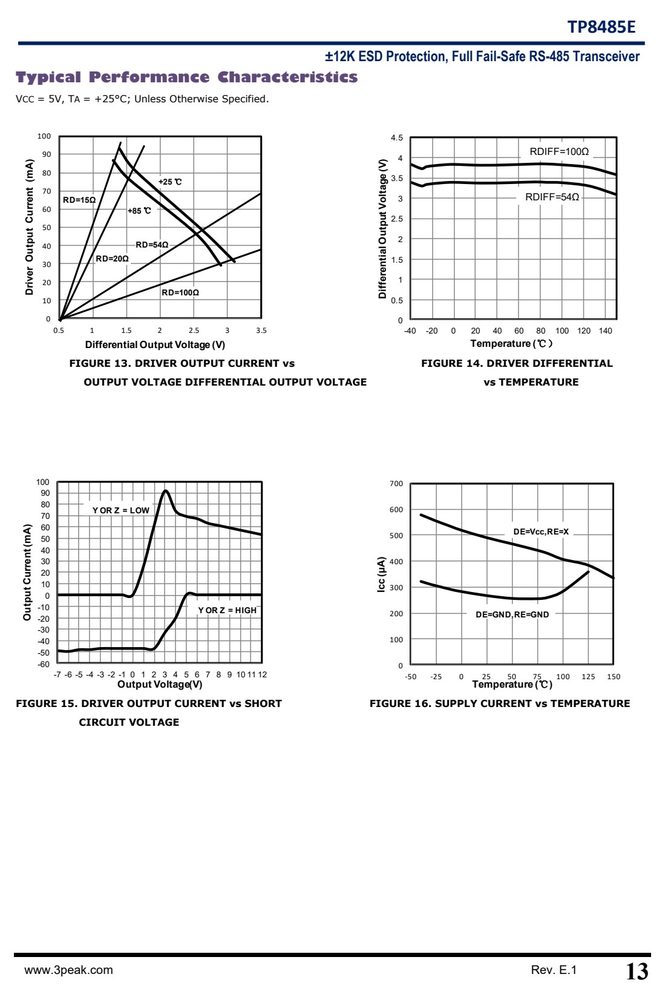
特性曲线(Typical Performance Curves)