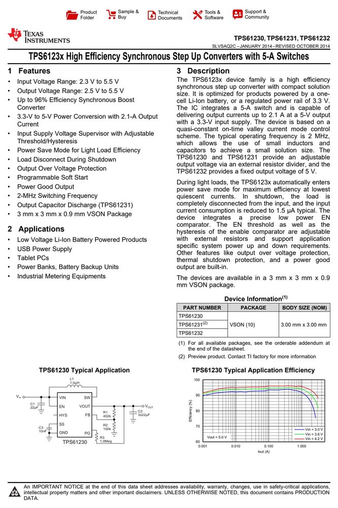
产品应用与封装尺寸
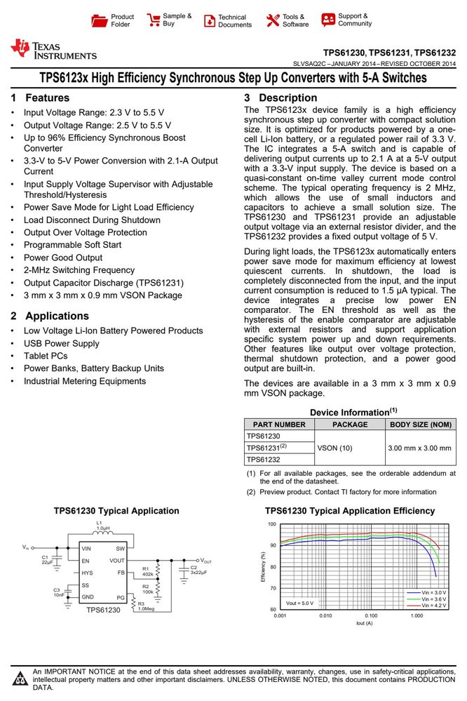
图纸取自原厂规格书,点击可放大查看原始尺寸标注。
引脚定义与内部结构
| 引脚 | 符号 | 名称 |
|---|---|---|
| 1 | SW | |
| 2 | SW | |
| 3 | VOUT | |
| 4 | VOUT | |
| 5 | PG |
数据来源:原厂规格书引脚图
产品特点 Features
- The TPS6123x device family is a high efficiency
- Input Voltage Range: 2.3 V to 5.5 V
- 1 synchronous step up converter with compact solution
- Output Voltage Range: 2.5 V to 5.5 V size. It is optimized for products powered by a one-
- Up to 96% Efficiency Synchronous Boost cell Li-Ion battery, or a regulated power rail of 3.3 V.
- Converter The IC integrates a 5-A switch and is capable of delivering output currents up to 2.1 A at a 5-V output
- 3.3-V to 5-V Power Conversion with 2.1-A Output with a 3.3-V input supply. The device is based on a
- Current quasi-constant on-time valley current mode control
- Input Supply Voltage Supervisor with Adjustable scheme. The typical operating frequency is 2 MHz,
- Threshold/Hysteresis which allows the use of small inductors and
- Power Save Mode for Light Load Efficiency capacitors to achieve a small solution size. The
- TPS61230 and TPS61231 provide an adjustable
- Load Disconnect During Shutdown output voltage via an external resistor divider, and the
- Output Over Voltage Protection
- TPS61232 provides a fixed output voltage of 5 V.
- Programmable Soft Start
绝对最大额定值 Absolute Maximum Ratings(TA = 25°C)
超过下表数值可能造成器件永久损坏,设计时请留余量。
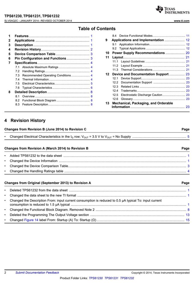
| 1 | 特性 | 12 | 8.4 | 器件 | Functional | Modes........................................ | 11 |
|---|---|---|---|---|---|---|---|
| 11.3 | Thermal | Considerations........................................ | 21 |
数据来源:原厂规格书
电气特性 Electrical Characteristics(TA = 25°C)
| 1 | 特性 | 12 | 8.4 | 器件 | Functional | Modes........................................ | 11 |
|---|---|---|---|---|---|---|---|
| 12.3 | Related | Links | ........................................................ | 23 |
特性曲线(Typical Performance Curves)