产品应用与封装尺寸
图纸取自原厂规格书,点击可放大查看原始尺寸标注。
引脚定义与内部结构
| 引脚 | 符号 | 名称 |
|---|---|---|
| 2 | MOSFET | |
| 3 | W | |
| 4 | A | |
| 5 | OUTB | |
| 6 | VDD | |
| 7 | OUTA | |
| 8 | ENBB |
数据来源:原厂规格书引脚图
关键参数速览
- 电源电压 VCC
- V Supply voltage -0.3 to 16
产品特点 Features
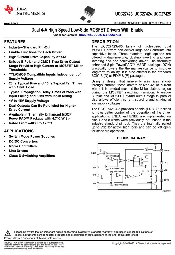
- The UCC27423/4/5 family of high-speed dual
- Industry-Standard Pin-Out
- 2 MOSFET drivers can deliver large peak currents into
- Enable Functions for Each Driver capacitive loads. Three standard logic options are
- High Current Drive Capability of ±4A offered – dual-inverting, dual-noninverting and one-
- Unique BiPolar and CMOS True Drive Output inverting and one-noninverting driver. The thermally enhanced 8-pin PowerPAD™ MSOP package (DGN)
- Stage Provides High Current at MOSFET Miller drastically lowers the thermal resistance to improve
- Thresholds
- UCC27423, UCC27424, UCC27425
- OUTPUT TEMPERATURE
- CONFIGURATION T = T
- Dual inverting –40°C to
- Dual nonInverting –40°C to
- One inverting, one
- –40°C to noninverting
- (1) D (SOIC-8) and DGN (PowerPAD-MSOP)
绝对最大额定值 Absolute Maximum Ratings(TA = 25°C)
超过下表数值可能造成器件永久损坏,设计时请留余量。
| 值 | 单位 |
|---|---|
| over operating free-air temperature range (unless otherwise noted) (1) | |
| V Supply voltage -0.3 to 16 | V |
| I Output current (OUTA, OUTB) DC 0.2 | A |
| I Pulsed, (0.5μs) 4.5 | A |
| V Input voltage (INA, INB) -5 to 6 or V +0.3 (whichever is | larger) V |
| Enable voltage (ENBA, ENBB) –0.3 V to 6 V or V +0.3 (whichever is | larger) |
| DGN package 3 | W |
| Power dissipation at T = 25°C D package 650 | |
| P package 350 | |
| T Junction operating temperature –55 to 150 | |
| T Storage temperature –65 to 150 | °C |
| Lead temperature (soldering, 10 sec) 300 |
数据来源:原厂规格书
电气特性 Electrical Characteristics(TA = 25°C)
| 参数 | 测试条件 | 最小 | 典型 | 最大 | 单位 |
|---|---|---|---|---|---|
| V Logic 1 input threshold | 2 | ||||
| V Logic 0 input threshold | 1 | ||||
| Input current | 0 V ≤ V ≤ V | –10 | 0 | 10 | μA |
| Output current | V = 14 V (1) | 4 | A | ||
| V High-level output voltage | V = V – V , I = –10 mA | 330 | 450 | ||
| V Low-level output level | I = 10 mA | 22 | 45 | ||
| T = 25°C, I = –10 mA, V = 14 V(2) | 25 | 30 | 35 | ||
| T = full range, I = –10 mA, V = 14 V(2) | 18 | 45 | |||
| T = 25°C, I = 10 mA, V = 14 V(2) | 1.9 | 2.2 | 2.5 | ||
| T = full range I = 10 mA, V = 14 V(2) | 1.2 | 4.0 | |||
| Latch-up protection | 500 | mA | |||
| t Rise time (OUTA, OUTB) | C = 1.8 nF | 20 | 40 | ||
| t Fall time (OUTA, OUTB) | C = 1.8 nF | 15 | 40 | ||
| t Delay, IN rising (IN to OUT) | C = 1.8 nF | 25 | 40 | ||
| t Delay, IN falling (IN to OUT) | C = 1.8 nF | 35 | 50 | ||
| V High-level input voltage | LO to HI transition | 1.7 | 2.4 | 2.9 | |
| V Low-level input voltage | HI to LO transition | 1.1 | 1.8 | 2.2 | V |
| Hysteresis | 0.15 | 0.55 | 0.90 | ||
| R Enable impedance | V = 14 V, ENBL = GND | 75 | 100 | 140 | kΩ |
| t Propagation delay time (see Figure 2) | C = 1.8 nF | 30 | 60 | ||
| t Propagation delay time (see Figure 2) | C = 1.8 nF | 100 | 150 | ||
| INA = 0 V, INB = 0 V | 900 | 1350 | |||
| UCC27423 | INA = 0 V, INB = HIGH | 750 | 1100 | μA | |
| INA = HIGH, INB = 0 V | 750 | 1100 | |||
| INA = HIGH, INB = HIGH | 600 | 900 | |||
| INA = 0 V, INB = 0 V | 300 | 450 | |||
| INA = 0 V, INB = HIGH | 750 | 1100 | |||
| I V = 15 V, UCC27424 | μA | ||||
| ENBA = ENBB = 15 V | INA = HIGH, INB = 0 V | 750 | 1100 | ||
| INA = HIGH, INB = HIGH | 1200 | 1800 | |||
| INA = 0 V, INB = 0 V | 600 | 900 | |||
| UCC27425 | INA = 0 V, INB = HIGH | 1050 | 1600 | μA | |
| INA = HIGH, INB = 0 V | 450 | 700 | |||
| INA = HIGH, INB = HIGH | 900 | 1350 | |||
| INA = 0 V, INB = 0 V | 300 | 450 | |||
| Disabled, V = 15 V, I DD All | INA = 0 V, INB = HIGH | 450 | 700 | μA | |
| DD ENBA = ENBB = 0 V | INA = HIGH, INB = 0 V | 450 | 700 | ||
| INA = HIGH, INB = HIGH 90% | 600 90% | 900 | |||
| t D1 t F t D2 | t f | t F | |||
| 90% | 90% | 90% | |||
| OUTPUT 10% | OUTPUT | 10% | t D2 |
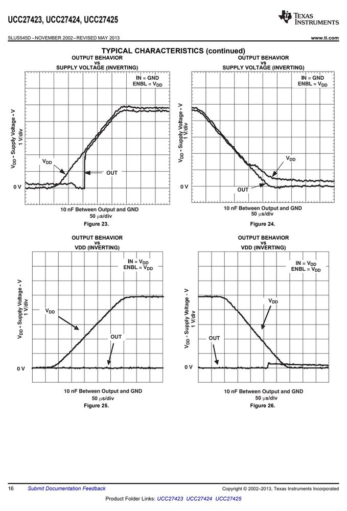
特性曲线(Typical Performance Curves)