
产品应用与封装尺寸
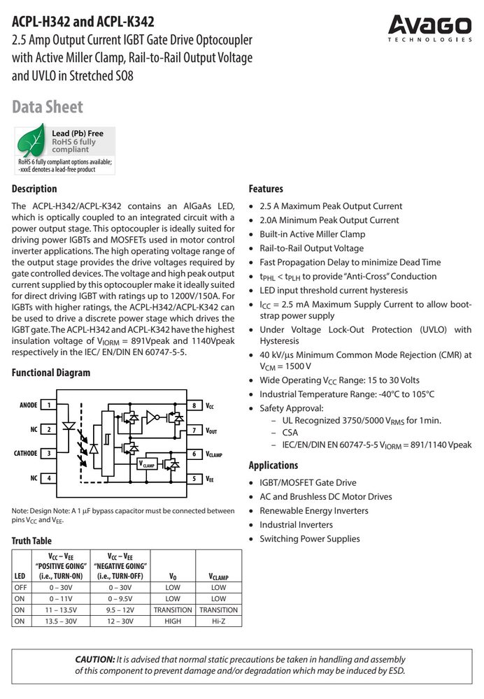
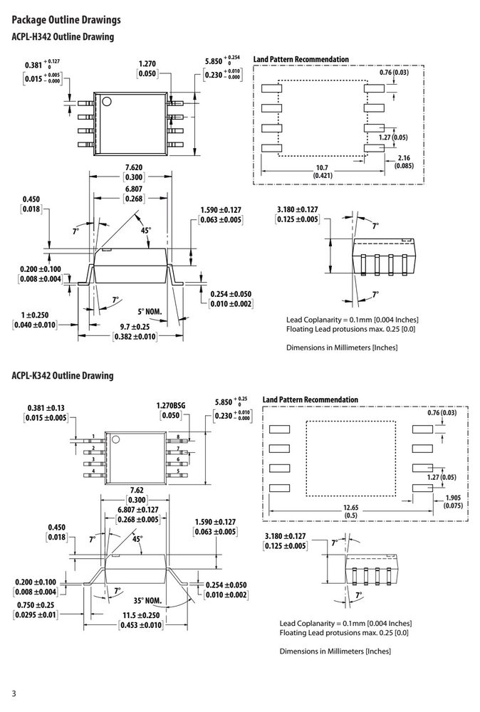
图纸取自原厂规格书,点击可放大查看原始尺寸标注。
引脚定义与内部结构
| 引脚 | 符号 | 名称 |
|---|---|---|
| 5 | V | |
| 6 | V | |
| 7 | V | |
| 8 | V |
数据来源:原厂规格书引脚图
关键参数速览
- 正向电压 VF
- 22
- 电源电压 VCC
- 35
- 工作温度 TA
- 105
产品特点 Features
- The ACPL-H342/ACPL-K342 contains an AlGaAs LED, which is optically coupled to an integrated circuit with a power output stage. This optocoupler is ideally suited for driving power IGBTs and MOSFETs used in motor control
- 2.5 A Maximum Peak Output Current
- 2.0A Minimum Peak Output Current
- Built-in Active Miller Clamp
- Rail-to-Rail Output Voltage clamp, Rail-to-Rail output voltage, Anti-cross conduction and LED input current hysteresis.
- Active Miller clamp function eliminates the need of negative gate drive in most application and allows the use of simple bootstrap supply for high side driver. Rail-to-
- Rail output voltage ensures that the IGBT’s gate voltage is driven to the optimum intended level with no power loss through between the high and low side of half bridge
- The supply bypass capacitors (1 µF) provide the large transient currents necessary during a switching transition.
- The gate resistor R serves to limit gate charge current and controls the IGBT collector voltage rise and fall times.
- voltage to the IGBT by forcing the ACPL-H342 output low during power-up. IGBTs typically require gate voltages of
- 15 V to achieve their rated V voltage. At gate voltages
- CE(ON) below 13 V typically, the V voltage increases dra-
- CC CC UVLO+ itive-going UVLO threshold), the UVLO clamp is released to allow the device output to turn on in response to input signals.
- Thermal Model for ACPL-H342/K342 Stretched SO8
- Package Optocoupler
- Definitions:
绝对最大额定值 Absolute Maximum Ratings(TA = 25°C)
超过下表数值可能造成器件永久损坏,设计时请留余量。
| 参数 | 符号 | 最小 | 最大 | 单位 | 备注 |
|---|---|---|---|---|---|
| Storage Temperature | T | -55 | 125 | °C | |
| Operating Temperature | T | -40 | 105 | °C | |
| Output IC Junction Temperature | T | 125 | °C | ||
| Average Input Current | I | 25 | mA | 1 | |
| Peak Transient Input Current | I | 1 | A | ||
| “High” Peak Output Current | I | 2.5 | A | 2 | |
| “Low” Peak Output Current | I | 2.5 | A | 2 | |
| Peak Clamp Sink Current | I | 2.5 | A | 2 | |
| Total Output Supply Voltage | (V - V ) | 0 | 35 | V | |
| Output Voltage | V | -0.5 | V | V | |
| Output IC Power Dissipation | P | 500 | mW | 3 | |
| Total Power Dissipation | P | 550 | mW | 4 | |
| Lead Solder Temperature | 260°C for 10 | sec., 1.6 mm below | seating plane |
数据来源:原厂规格书
安全与绝缘额定值(DIN EN/IEC 60747−5−5)
| 说明 | 符号 | 包装 | 060 | 包装2 | 0602 | 单位 |
|---|---|---|---|---|---|---|
| ISO RMS | ISO | RMS | ||||
| ACPL-H342 | ACPL-K342 | |||||
| for rated mains voltage ≤ 150 V rms | I – | IV | I – | IV | ||
| for rated mains voltage ≤ 300 V rms | I – | IV | I – | IV | ||
| for rated mains voltage ≤ 450 V rms | I – | III | I – | IV | ||
| for rated mains voltage ≤ 600 V rms | I – | III | I – | IV | ||
| for rated mains voltage ≤ 1000 V rms | I – | III | ||||
| Pollution Degree (DIN VDE 0110/39) | 2 | 2 | ||||
| Input to Output Test Voltage, Method b* | V | 1671 | 2137 | V | ||
| Input to Output Test Voltage, Method a* | V | 1426 | 1824 | V | ||
| Highest Allowable Overvoltage* | V | 6000 | 8000 | V | ||
| Case Temperature | T | 175 | 175 | °C | ||
| Input Current | I | 230 | 230 | mA | ||
| Output Power | P | 600 | 600 | mW | ||
| Insulation Resistance at T S , V IO = 500 V | R S | >109 | >109 | W |
电气特性 Electrical Characteristics(TA = 25°C)
| 参数 | 符号 | 最小 | 典型 | 最大 | 单位 | 测试条件 | 图号 | 备注 |
|---|---|---|---|---|---|---|---|---|
| A | F(ON) | F(OFF) | CC | |||||
| High Level Peak Output | Current I OH | -0.5 | -1.2 | A | V = V – 4 O CC | 3, 4, 23 | 5 | |
| -2.0 | A | V = V – 15 | 2 | |||||
| Low Level Peak Output | Current I OL | 0.5 | 2.7 | A | V = V + 2.5V O EE | 6, 7, 24 | 5 | |
| 2.0 | A | V = V + 15V | 2 | |||||
| High Output Transistor | RDS(ON) R DS,OH | 2.6 | 5.0 | W | I OH = -2.0A | 8 | ||
| Low Output Transistor | RDS(ON) R DS,OL | 0.8 | 2.0 | W | I OL = 2.0A | 9 | ||
| Clamp Output Peak | Current I CLAMP | 1.0 | 2.5 | A | V = V + 2.5 O EE | 14, 16, | 2 | |
| Clamp Pin Threshold | V | 2.3 | V | 15,16, | ||||
| Clamp Output Transistor | R DS,CLAMP | 0.8 | 2.0 | W | I CLAMP = 1.5 A | |||
| High Level Output | Voltage V | V -2.0 | V -0.80 | V | I = -100 mA | 2, 4, 25 | 6, 7 | |
| OH | CC | CC | O | |||||
| High Level Output | Voltage V | V | V | I = 0 mA , I =10 | mA 1 | |||
| OH | CC | O F | ||||||
| Low Level Output | Voltage V | 0.07 | 0.25 | V | I = 100 mA | 5, 7, 26 | ||
| High Level Supply | Current I | 1.68 | 2.5 | mA | R = 10W, | 10, 11 | ||
| C = 25 nF, I = 10 | mA, | |||||||
| Low Level Supply Current | I | 2.0 | 2.5 | mA | R = 10W, | |||
| C = 25 nF, I = 0 | mA | |||||||
| Threshold Input Current | I | 0.5 | 1.5 | 4.0 | mA | R = 10W, | 12, 13, | |
| Low to High | C = 25 nF, V > 5 | V 29 | ||||||
| Threshold Input Voltage | V | 0.8 | V | |||||
| Input Forward Voltage | V | 1.2 | 1.55 | 1.95 | V | I = 10 mA | 22 | |
| Temperature Coefficient | of ΔV /ΔT | -1.7 | mV/°C | |||||
| Input Capacitance | C | 70 | pF | f = 1 MHz, V = 0 V | ||||
| UVLO Threshold | V UVLO+ | 11.0 | 12.3 | 13.5 | V | V > 5 V, I = 10 mA O F | 30 | |
| V | 9.5 | 10.7 | 12.0 |
相关 / 可替代型号
以上型号来自规格书与型号命名比对,参数需以各自规格书为准;下单前请与销售确认封装与脚位。
订货信息与供货形式
| 型号 | 型号2 | (RoHS | Compliant) | 封装 | Mount | 包装 | Minute | 额定值 | 60747-5-5 | 数量 |
|---|---|---|---|---|---|---|---|---|---|---|
| column | to | form an | order entry. |