
产品应用与封装尺寸
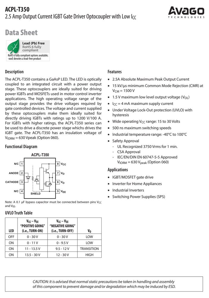
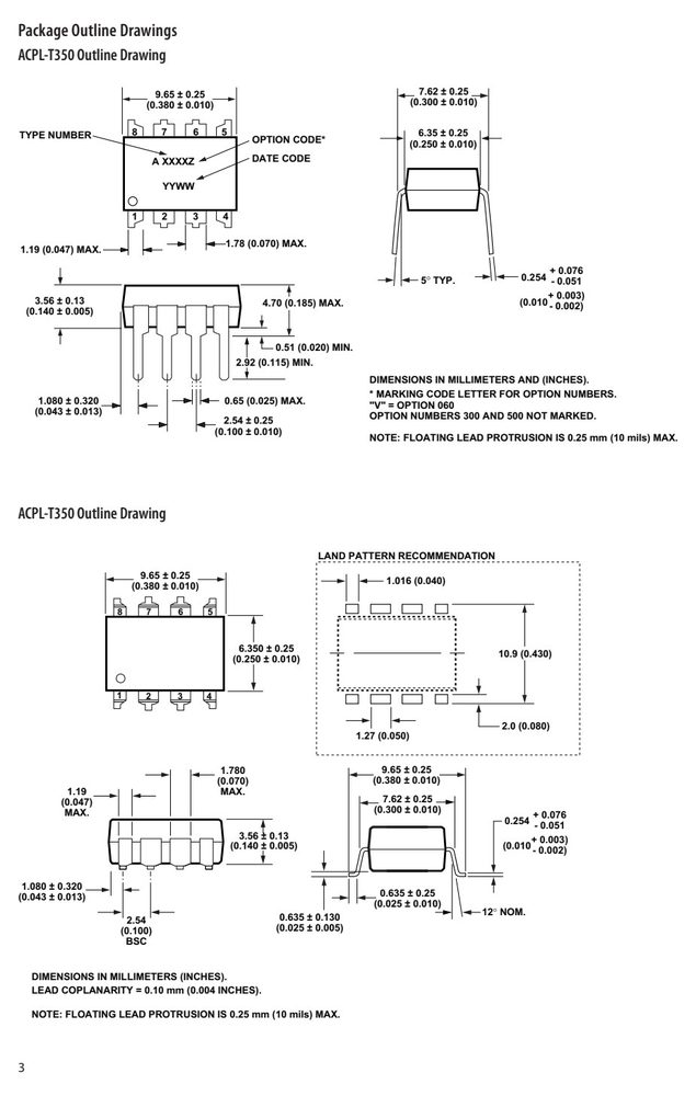
图纸取自原厂规格书,点击可放大查看原始尺寸标注。
引脚定义与内部结构
| 引脚 | 符号 | 名称 |
|---|---|---|
| 4 | V | |
| 5 | VEE | |
| 6 | VO | |
| 7 | VO | |
| 8 | VCC |
数据来源:原厂规格书引脚图
关键参数速览
- 正向电压 VF
- 1.8
- 隔离电压 VISO
- 4500 Vrms for 1
- 工作温度 TA
- 100
产品特点 Features
- The ACPL-T350 contains a GaAsP LED. The LED is optically • 2.5A Absolute Maximum Peak Output Current coupled to an integrated circuit with a power output
- 15 kV/µs minimum Common Mode Rejection (CMR) at stage. These optocouplers are ideally suited for driving
- V = 1500 V power IGBTs and MOSFETs used in motor control inverter
- 1.5 V maximum low level output voltage (V )
绝对最大额定值 Absolute Maximum Ratings(TA = 25°C)
超过下表数值可能造成器件永久损坏,设计时请留余量。
| 参数 | 符号 | 最小 | 最大 | 单位 | 备注 |
|---|---|---|---|---|---|
| Storage Temperature | T | -55 | 125 | °C | |
| Operating Temperature | T | -40 | 100 | °C | |
| Average Input Current | I | 25 | mA | 1 | |
| Peak Transient Input Current | I | 1.0 | A | ||
| “High” Peak Output Current | I | 2.5 | A | 2 | |
| “Low” Peak Output Current | I | 2.5 | A | 2 | |
| Supply Voltage | V – V | 0 | 35 | V | |
| Input Current (Rise/Fall | Time) t /t | 500 | ns | ||
| Output Voltage | V | 0 | V | V | |
| Output Power Dissipation | P | 250 | mW | 3 | |
| Total Power Dissipation | P | 295 | mW | 4 | |
| Lead Solder Temperature | 260°C for 10 | sec., 1.6 mm below | seating plane |
数据来源:原厂规格书
安全与绝缘额定值(DIN EN/IEC 60747−5−5)
| 说明 | 符号 | 包装 | 060 | 单位 |
|---|---|---|---|---|
| ACPL-T350 | ||||
| Installation classification per DIN VDE 0110/39, | Table 1 | |||
| for rated mains voltage ≤ 150 V | I – IV | |||
| for rated mains voltage ≤ 300 V | I – IV | |||
| for rated mains voltage ≤ 450 V | I – III | |||
| Pollution Degree (DIN VDE 0110/39) | 2 | |||
| Input to Output Test Voltage, Method b* | V | 1181 | V | |
| V x 1.875=V , 100% Production Test with | t =1 sec, Partial discharge < 5 pC | |||
| Input to Output Test Voltage, Method a* | V | 1008 | V | |
| V x 1.6=V , Type and Sample Test, t =10 | sec, Partial discharge < 5 pC | |||
| Highest Allowable Overvoltage (Transient | Overvoltage t = 60 sec) V ini IOTM | 6000 | V peak | |
| Case Temperature | T | 175 | °C | |
| Input Current | I | 230 | mA | |
| Output Power | P | 600 | mW | |
| Insulation Resistance at T , V = 500 V | R | >109 | W | |
| ACPL-T350 | Option 060 | |||
| detailed description of Method a and Method b partial | discharge test profiles. | |||
| Surface mount classification is Class A in accordance | with CECC 00802. 600 - 400 | |||
| 0 | 25 50 | 75 100 | 125 150 175 | |
| T - CASE | TEMPERATURE | - °C | ||
| Gap (Clearance) | through air. | |||
| Tracking (Creepage) | path along body. | |||
| Minimum Internal 0.08 | mm Through insulation distance conductor | to | conductor, | usually the |
| Plastic Gap | straight line distance thickness between | the | emitter | and detector. |
| Tracking Resistance CTI > 175 | V DIN IEC 112/VDE 0303 Part 1 | |||
| Isolation Group IIIa | Material Group (DIN VDE 0110, 1/89, | Table 1) |
电气特性 Electrical Characteristics(TA = 25°C)
| 参数 | 符号 | 最小 | 典型 | 最大 | 单位 | 测试条件 | 图号 | 备注 |
|---|---|---|---|---|---|---|---|---|
| A | F(ON) | F(OFF) | CC | |||||
| EE | A | CC | EE | |||||
| High Level Output | Current I OH | 0.5 | 1.6 | A | V = V – 4 V O CC | 2, 3, 15 | 5 | |
| 2.0 | A | V = V – 15 V | 2 | |||||
| Low Level Output Current | I OL | 0.5 | 1.6 | A | V = V + 2.5 V O EE | 5, 6, 16 | 5 | |
| 2.0 | A | V = V + 15 V | 2 | |||||
| High Level Output Voltage | V | V -4 | V -3 | V | I = -100 mA | 1, 3, 17 | 6, 7 | |
| OH | CC | CC | O | |||||
| Low Level Output Voltage | V | V +0.5 | 1.5 | V | I = 100 mA | 4, 6, 18 | ||
| OL | EE | O | ||||||
| High Level Supply Current | I | 2.0 | 4.0 | mA | Output open, | 7, 8 | ||
| I = 7 to 16 mA | ||||||||
| Low Level Supply Current | I | 2.0 | 4.0 | mA | Output open, | |||
| V = -3.0 to +0.8 | V | |||||||
| Threshold Input Current | I FLH | 2.0 | 5 | mA | I = 0 mA, V > O O | 5 V 9, 19 | ||
| Threshold Input Voltage | V FHL | 0.8 | V | I = 0 mA, V > O O | 5 V | |||
| Input Forward Voltage | V | 1.2 | 1.5 | 1.8 | V | I = 10 mA | ||
| Temperature Coefficient | DV /DT | -2.0 | mV/°C | I = 10 mA | ||||
| Input Capacitance | C | 60 | pF | f = 1 MHz, V = 0 | V | |||
| UVLO Threshold | V UVLO+ | 11.0 | 12.3 | 13.5 | V | I = 10 mA, V > F O | 5 V 14, 20 | |
| V UVLO– | 9.5 | 10.7 | 12.0 | V | I = 10 mA, V > F O | 5 V | ||
| UVLO Hysteresis | UVLO HYS | 1.6 | V | I = 10 mA, V > F O | 5 V | |||
| Input-Output Momentary | Withstand V | 3750 | Vrms | RH < 50%, | 14, 15 | |||
| Voltage** | t = 1 min., T = 25°C | |||||||
| Resistance Input-Output) | R | 1012 | W | V = 500 V | 15 | |||
| Capacitance Input-Output) | C | 0.6 | pF | Freq=1 MHz | ||||
| LED-to-Case Thermal | Resistance q | 467 | °C/W | Thermocouple | located | |||
| at center underside | of | |||||||
| LED-to-Detector Thermal | Resistance q | 442 | °C/W | |||||
| Detector-to-Case Thermal | Resistance q | 126 | °C/W | |||||
| 1. Derate linearly above 70°C | free-air temperature at a rate | of 0.3 mA | /°C. | |||||
| 3. Derate linearly above 70° C | free-air temperature at a rate | of 4.8 | mW /°C. | |||||
| 9. Pulse Width Distortion (PWD) | is defined as |tPHL - tPLH| | for any given | device. |
特性曲线(Typical Performance Curves)
订货信息与供货形式
| 型号 | 型号2 | Compliant | 封装 | Surface | Mount | Gull | Wing | Tape& | 包装 | 60747-5-5 | 数量 |
|---|---|---|---|---|---|---|---|---|---|---|---|
| ACPL-T350 | is UL | Recognized | with 3750 Vrms | for 1 | minute per | UL1577. | |||||
| Part | number | Compliant | Package | Surface | Mount | Gull | Wing | Tape& | Reel | 60747-5-5 | Quantity |
| RoHS | compliant | option will use | ‘-XXXE‘. | ||||||||
| The | ACPL-T350 | is approved by | the following | organizations: | |||||||
| Approval | under: | Approval | under | UL | 1577, | component | recognition | ||||
| DIN | EN 60747-5-5 | (VDE | 0884-5):2011-11 | program, | File | E55361. |