
产品应用与封装尺寸
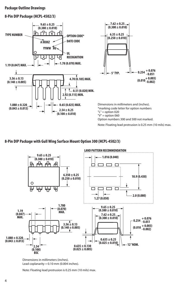
图纸取自原厂规格书,点击可放大查看原始尺寸标注。
引脚定义与内部结构
| 引脚 | 符号 | 名称 |
|---|---|---|
| 4 | RECOGNITION | |
| 5 | GND | |
| 6 | V | |
| 7 | NC | |
| 8 | V |
数据来源:原厂规格书引脚图
关键参数速览
- 电流传输比 CTR
- 5
- 正向电流 IF
- 60747-5-5
- 隔离电压 VISO
- 60747-5-5
- 电源电压 VCC
- 30
- 工作温度 TA
- 100
产品特点 Features
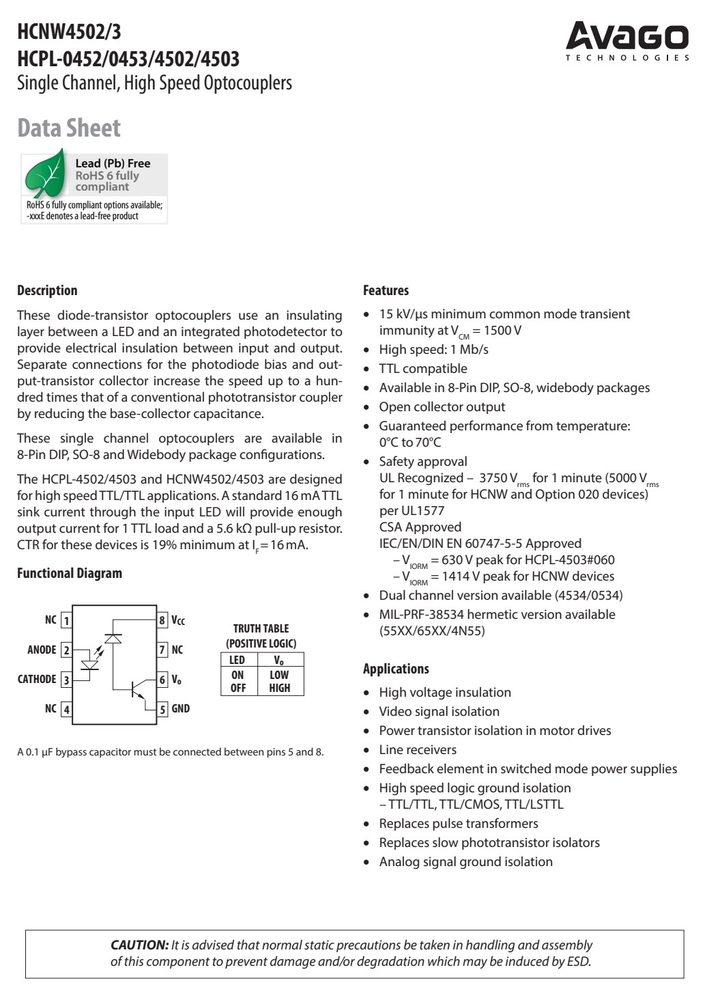
- These diode-transistor opto coup lers use an insulating layer between a LED and an integrated photodetector to provide elec trical in su lation between input and out put.
- Separate connections for the photodiode bias and out- put-transistor collector increase the speed up to a hun- dred times that of a conven tional phototransistor coupler by reduci ng the base-collector capacitance.
- These single channel optocoupl ers are available in
- 8-Pin DIP , SO-8 and Widebody package configurations.
- 15 kV/µs minimum common mode transient immunity at V = 1500 V
- High speed: 1 Mb/s
- TTL compatible
- Available in 8-Pin DIP, SO-8, widebody packages
- Open collector output
- Guaranteed performance from temperature:
- 0°C to 70°C
- The HCPL-4502, HCPL-0452, and HCNW4502 provide the Schematic
绝对最大额定值 Absolute Maximum Ratings(TA = 25°C)
超过下表数值可能造成器件永久损坏,设计时请留余量。
| 参数 | 符号 | 器件 | 最小 | 最大 | 单位 | 备注 |
|---|---|---|---|---|---|---|
| Storage Temperature | T | -55 | 125 | °C | ||
| Operating Temperature | T | 8-Pin DIP | -55 | 100 | °C | |
| Widebody | -55 | 85 | ||||
| Average Forward Input Current | I | 25 | mA | 1 | ||
| Peak Forward Input Current | I | 8-Pin DIP | 2 | |||
| (50% duty cycle, 1 ms pulse width) | SO-8 | 50 | mA | |||
| (50% duty cycle, 1 ms pulse width) | Widebody | 40 | ||||
| Peak Transient Input Current | I | 8-Pin DIP Widebody Widebody | 1 0.1 3 | A | ||
| Input Power Dissipation | P | 8-Pin DIP Widebody | 45 40 | mW | 3 | |
| Average Output Current (Pin 6) | I | 8 | mA | |||
| Peak Output Current | I | 16 | mA | |||
| Supply Voltage (Pin 8-5) | V | -0.5 | 30 | V | ||
| Output Voltage (Pin 6-5) | V | -0.5 | 20 | V | ||
| Base Current (Pin 7, except 4502/3, | 0452/3) I | 5 | mA | |||
| Output Power Dissipation | P | 100 | mW | 4 | ||
| 1.6 mm below seating plane, 10 | seconds T | 8-Pin DIP | 260 | °C | ||
| up to seating plane, 10 seconds | Widebody | 260 | °C |
数据来源:原厂规格书
安全与绝缘额定值(DIN EN/IEC 60747−5−5)
| 说明 | 符号 | HCPL-4502/4503 | HCPL-0452/0453 | 单位 |
|---|---|---|---|---|
| Input to Output Test Voltage, Method | b* | |||
| V x 1.875 = V , 100% Production | Test with t = 1 sec, V | 1181 | 1050 | V |
| IORM PR | m PR | peak | ||
| Input to Output Test Voltage, Method | a* | |||
| V x 1.6 = V , Type and sample | test, V | 1008 | 896 | V |
| IORM PR | PR | peak | ||
| t = 10 sec, Partial Discharge < 5 | pC | |||
| (Transient Overvoltage, t = 60 sec) | V | 8000 | 6000 | V |
| ini | IOTM | peak | ||
| Input to Output Test Voltage, Method | b* | |||
| V x 1.875 = V , 100% Production | Test with t = 1 sec, | V | 2652 | V |
| IORM PR | m | PR | peak | |
| Input to Output Test Voltage, Method | a* | |||
| V x 1.6 = V , Type and sample | test, | V | 2262 | V |
| IORM PR | PR | peak | ||
| t = 10 sec, Partial Discharge < 5 | pC | |||
| (Transient Overvoltage, t = 60 sec) | V | 8000 | V | |
| ini | IOTM | peak |
电气特性 Electrical Characteristics(TA = 25°C)
| 参数 | 符号 | 器件 | 最小 | Typ.* | 最大 | 单位 | 测试条件 | 图号 | 备注 |
|---|---|---|---|---|---|---|---|---|---|
| Over | recommended | temperature | (T = 0°C | to 70°C) | unless | otherwise | specified. See note 13. | ||
| Current | CTR | HCPL-4502/3 | 19 | 24 | 50 | % | T = 25°C V = 0.4 V A O | I = 16 mA, 1, 2, F | 5 |
| Transfer Ratio | HCPL-0452/3 | 15 | 24 | V = 0.5 V | V = 4.5 V 4 | ||||
| Logic Low | V | HCPL-4502/3 | 0.1 | 0.4 | V | T = 25°C I = 3.0 mA | I = 16 mA, | ||
| OL | A O | F | |||||||
| Output Voltage | HCPL-0452/3 | 0.1 | 0.5 | I = 2.4 mA | V = 4.5 V | ||||
| Logic High | I | 0.003 | 0.5 | µA | T = 25°C V = V = 5.5 V | I = 0 mA 7 | |||
| OH | A O CC | F | |||||||
| Output Current | 0.01 | 1 | T = 25°C V = V = 15 V | ||||||
| 50 | V = V = 15 V | ||||||||
| Logic Low | I CCL | 50 | 200 | µA | I = 16 mA, V = Open, F O | 10 | |||
| Supply Current | V = 15 V | ||||||||
| Logic High | I CCH | 0.02 | 1 2 | µA | T = 25°C I = 16 mA, A F V = 15 V | 10 | |||
| Input Forward | V F | 8-Pin DIP | 1.5 | 1.7 | V | T = 25°C I = 16 mA A F | 3 | ||
| Widebody | 1.45 | 1.68 | 1.85 | T = 25°C I = 16 mA | |||||
| Voltage | Widebody | 3 | I = 100 | ||||||
| Temperature | ∆V / | 8-Pin DIP | -1.6 | mV/°C | I = 16 mA | ||||
| Input | C | 8-Pin DIP | 60 | pF | f = 1 MHz, V = 0 V | ||||
| Transistor DC | h FE | 8-Pin DIP | 150 | V = 5 V, I = 3 mA O O | |||||
| Current Gain | SO-8 | 130 | V = 0.4 V, I = 20 µA | ||||||
| Widebody | 180 | V = 0.4 V, I = 20 µA | |||||||
| 160 | V = 5 V, I = 3 mA | ||||||||
| Over recommended | temperature | (T = 0°C | to 70°C) | unless | otherwise | specified. | |||
| Input-Output | V | 8-Pin DIP | 3750 | V rms | RH < 50%, | 6, 11 | |||
| Momentary | SO-8 | t = 1 min., | |||||||
| Widebody | 5000 | T = 25°C | 6, 12 | ||||||
| 8-Pin DIP | 5000 | 6, 9, | |||||||
| (Option 020) | 12 | ||||||||
| I | 8-Pin DIP | 1 | µA | 45% RH, t = 5 s, V = 3 kVdc, T = 25°C | 6, 13 | ||||
| Input-Output | R | 8-Pin DIP | 1012 | Ω | V = 500 Vdc | 6 | |||
| Widebody | 1012 | 1013 | T = 25°C | ||||||
| 1011 | T = 100°C | ||||||||
| Input-Output | C | 8-Pin DIP | 0.6 | pF | f = 1 MHz | 6 | |||
| 1. Derate linearly | above 70°C free-air | temperature | at a rate of 0.8 | mA/°C (8-Pin | DIP). | ||||
| Derate linearly | above 85°C free-air | temperature | at a rate of 0.5 | mA/°C (SO-8). | |||||
| 2. Derate linearly | above 70°C free-air | temperature | at a rate of 1.6 | mA/°C (8-Pin | DIP). | ||||
| Derate linearly | above 85°C free-air | temperature | at a rate of 1.0 | mA/°C (SO-8). | |||||
| 3. Derate linearly | above 70°C free-air | temperature | at a rate of 0.9 | mW/°C (8-Pin | DIP). | ||||
| Derate linearly | above 85°C free-air | temperature | at a rate of 1.1 | mW/°C (SO-8). | |||||
| 4. Derate linearly | above 70°C free-air | temperature | at a rate of 2.0 | mW/°C (8-Pin | DIP). | ||||
| Derate linearly | above 85°C free-air | temperature | at a rate of 2.3 | mW/°C (SO-8). | |||||
| output will remain | in a Logic Low | state (i.e., V < | 0.8 V). |
相关 / 可替代型号
以上型号来自规格书与型号命名比对,参数需以各自规格书为准;下单前请与销售确认封装与脚位。
订货信息与供货形式
| 3.937 | ± | 0.127 | YWW | 型号 | 型号2 | 7.49 | (0.295) |
|---|---|---|---|---|---|---|---|
| Small | Outline | SO-8 | Package (HCPL-0452/3) | ||||
| Lead | coplanarity | = 0.10 | mm (0.004 inches) | max. |