
产品应用与封装尺寸
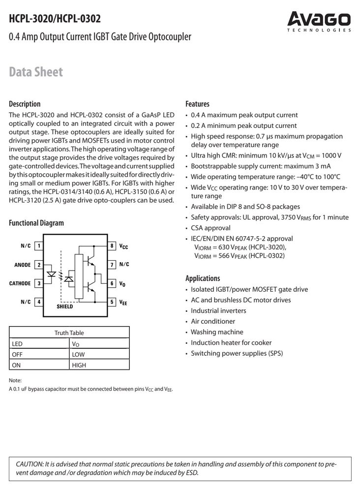
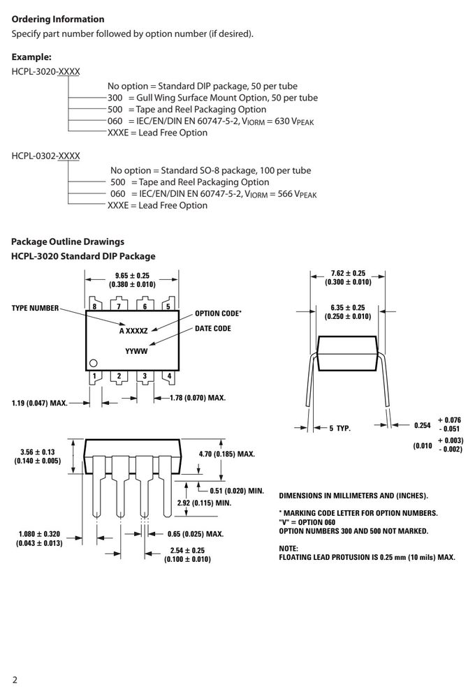
图纸取自原厂规格书,点击可放大查看原始尺寸标注。
引脚定义与内部结构
| 引脚 | 符号 | 名称 |
|---|---|---|
| 5 | V | |
| 6 | V | |
| 7 | N/C | |
| 8 | V |
数据来源:原厂规格书引脚图
关键参数速览
- 正向电压 VF
- 14
- 电源电压 VCC
- 35
- 工作温度 TA
- 100
产品特点 Features
- The HCPL-3020 and HCPL-0302 consist of a GaAsP LED • 0.4 A maximum peak output current optically coupled to an integrated circuit with a power
- 0.2 A minimum peak output current output stage. These optocouplers are ideally suited for
- High speed response: 0.7 µs maximum propagation driving power IGBTs and MOSFETs used in motor control delay over temperature range
- HCPL-3020 Gull Wing Surface Mount Option 300
- Land Pattern Recommendation
- 9.65 ± 0.25
- (0.380 ± 0.010) 1.016 (0.040)
- 8 7 6 5
- 6.350 ± 0.25
- (0.250 ± 0.010)
- 10.9 (0.430)
- 1 2 3 4
- 1.27 (0.050) 2.0 (0.080)
- 1.780 9.65 ± 0.25
- (0.070) (0.380 ± 0.010)
- 1.19 MAX.
绝对最大额定值 Absolute Maximum Ratings(TA = 25°C)
超过下表数值可能造成器件永久损坏,设计时请留余量。
| 参数 | 符号 | 最小 | 最大 | 单位 | 备注 |
|---|---|---|---|---|---|
| Storage Temperature | T | –55 | 125 | °C | |
| Operating Temperature | T | –40 | 100 | °C | |
| Average Input Current | I | 20 | mA | 1 | |
| Peak Transient Input Current (<1 µs | pulse width, 300 pps) I | 1.0 | A | ||
| “High” Peak Output Current | I | 0.4 | A | 2 | |
| “Low” Peak Output Current | I | 0.4 | A | 2 | |
| Supply Voltage | V – V | –0.5 | 35 | V | |
| Output Voltage | V | –0.5 | V | V | |
| Output Power Dissipation | P | 250 | mW | 3 | |
| Input Power Dissipation | P | 45 | mW | 4 | |
| Lead Solder Temperature | 260°C for | 10 sec., 1.6 | mm below | seating plane |
数据来源:原厂规格书
安全与绝缘额定值(DIN EN/IEC 60747−5−5)
| 说明 | 符号 | HCPL-3020 | HCPL-0302 | 单位 |
|---|---|---|---|---|
| V x 1.875 = V , 100% Production | Test with t = 1 sec, | |||
| Partial Discharge < 5 pC | V | 1181 | 1050 | V |
| V x 1.5 = V , Type and Sample Test, | t = 60 sec, | |||
| Partial Discharge < 5 pC | V | 945 | 840 | V |
| (Transient Overvoltage t = 10 sec) | V | 6000 | 4000 | V |
| ini | IOTM | peak |
电气特性 Electrical Characteristics(TA = 25°C)
| 参数 | 符号 | 最小 | 典型 | 最大 | 单位 | 测试条件 | 图号 |
|---|---|---|---|---|---|---|---|
| Over recommended | operating conditions unless | otherwise | specified. | ||||
| High Level Output Current | I OH | 0.15 | A | V = V – 4 O CC | 5 | ||
| 0.2 | 0.3 | A | V = V – 10 | 2 2 | |||
| Low Level Output Current | I OL | 0.15 | A | V = V + 2.5 O EE | 5 | ||
| 0.2 | 0.3 | A | V = V + 10 | 4 2 | |||
| High Level Output Voltage | V | V – 4 | V – 1.8 | V | I = –100 mA | 1 6, 7 | |
| OH | CC | CC | O | ||||
| Low Level Output Voltage | V | 0.4 | 1 | V | I = 100 mA | 3 | |
| High Level Supply Current | I | 0.7 | 3 | mA | I = 0 mA | 5, 6 14 | |
| Low Level Supply Current | I | 1.2 | 3 | mA | I = 0 mA | ||
| Threshold Input Current Low | to High I | 6 | mA | I = 0 mA, V > 5 V | 7, 13 | ||
| Threshold Input Voltage | High to Low V | 0.8 | V | ||||
| Input Forward Voltage | V | 1.2 | 1.5 | 1.8 | V | I = 10 mA | 14 |
| Temperature Coefficient of | Input DV /DT | –1.6 | mV/°C | ||||
| Input Capacitance | C | 60 | pF | f = 1 MHz, V = 0 V |