
产品应用与封装尺寸
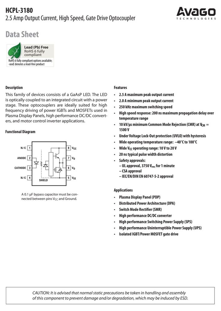
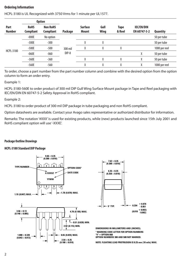
图纸取自原厂规格书,点击可放大查看原始尺寸标注。
引脚定义与内部结构
| 引脚 | 符号 | 名称 |
|---|---|---|
| 5 | VEE | |
| 6 | VO | |
| 7 | VO | |
| 8 | VCC |
数据来源:原厂规格书引脚图
关键参数速览
- 正向电压 VF
- 16
产品特点 Features
- The HCPL-3180 contains an under voltage lockout (UVLO)
- The HCPL-3180 includes a Propagation Delay Difference conditions which cause the HCPL-3180 supply voltage
- (equivalent to the fully charged IGBT gate voltage) to drop below a level necessary to keep the IGBT in a low resistance state. When the HCPL-3180 output is in the high state and the supply voltage drops below the HCPL-
- 3180 V threshold (typ 7.5 V) the optocoupler output
- UVLO- will go into the low state. When the HCPL-3180 output is in the low state and the supply voltage rises above the
- HCPL-3180 V threshold (typ 8.5 V) the optocoupler
- UVLO+ output will go into the high state (assume LED is “ON”).
- EGATLOV 14
- TUPTUO
- V O 4
- 0 5 10 15 20
- To minimize dead time in a given design, the turn on of
- LED2 should be delayed (relative to the turn off of LED1) so that under worst-case conditions, transistor Q1 has just turned off when transistor Q2 turns on, as shown in
- Figure 34. The amount of delay necessary to achieve this condition is equal to the maximum value of the propa- gation delay difference specification, PDD , which is
- MAX specified to be 90 ns over the operating temperature range of -40 °C to +100 °C.
- ILED1
绝对最大额定值 Absolute Maximum Ratings(TA = 25°C)
超过下表数值可能造成器件永久损坏,设计时请留余量。
| 参数 | 符号 |
|---|---|
| (<1 µs pulse width, 300 pps) | |
| Lead Solder Temperature | 260°C for 10 sec., |
| Solder Reflow Temperature | Profile See Package -55 125 °C -40 125 °C 25 mA 1 5 V -0.5 25 V 0 V V 250 mW 3 295 mW 4 |
| CLEDP 1 2 3 4 2 4 1 2 3 Q1 4 1 2 3 4 | µF + VCC = 20 V 8 7 6 5 7 5 8 7 6 CLEDN 5 8 7 6 5 |
数据来源:原厂规格书
安全与绝缘额定值(DIN EN/IEC 60747−5−5)
| 参数 | 符号 | 最小 | 典型 | 最大 | 单位 | 条件 | 图号 | 备注 |
|---|---|---|---|---|---|---|---|---|
| Input-Output Resistance | R | 10[11] | Ω | V = 500 V | 9 | |||
| Input-Output Capacitance | C | 1 | pF | Freq = 1 MHz | ||||
| 1. Derate linearly above | +70°C free air temperature | at a rate of | 0.3 mA/°C. | |||||
| minimum = 2.0 A. See | Application section for | additional | details on limiting | IOL peak. | ||||
| 3. Derate linearly above | +70°C, free air temperature | at the rate | of 4.8 mW/°C. |
电气特性 Electrical Characteristics(TA = 25°C)
| 参数 | 符号 | 最小 | 典型 | 最大 | 单位 | 条件 | 图号 | 备注 |
|---|---|---|---|---|---|---|---|---|
| Over recommended | operating conditions | unless | otherwise | specified. | ||||
| High Level Output | Current I | 0.5 | A | V = V - 4 | 2, 3, 17 | 5 | ||
| 2.0 | A | V = V -10 | 2, 3, 17 | 2 | ||||
| Low Level Output | Current I | 0.5 | A | V = V +2.5 | 5, 6, 18 | 5 | ||
| 2.0 | A | V = V +10 | 5, 6, 18 | 2 | ||||
| High Level Output | Voltage V V | -4 | V | I = -100 | mA 1, 3, 19 | 6, 7 | ||
| OH | CC | O | ||||||
| Low Level Output | Voltage V | 0.5 | V | I = 100 mA | 4, 6, 20 | |||
| High Level Supply | Current I | 3.0 | 6.0 | mA | Output Open | 7, 8 | ||
| I | = 10 to 16 | mA | ||||||
| Low Level Supply | Current I | 3.0 | 6.0 | mA | Output Open | 7, 8 | ||
| V | = 3.0 to | 0.8 mA | ||||||
| Threshold Input | Current I | 8.0 | mA | |||||
| Low to High | I = 0 mA, | 9, 15, 21 | ||||||
| Threshold Input | Voltage V | 0.8 | V | V > 5 V | ||||
| Input Forward Voltage | V | 1.2 | 1.5 | 1.8 | V | I = 10 mA | 16 | |
| Temperature Coefficient | of DV /DT | –1.6 | mV/°C | I = 10 mA | ||||
| UVLO Threshold | V | 7.9 | V | I = 10 mA, | ||||
| V | 7.4 | V | V > 5 V | 22, 33 | ||||
| UVLO Hysteresis | UVLO | 0.5 | V | |||||
| Input Capacitance | C | 60 | pF V | f = 1 MHz, = 0 V |
相关 / 可替代型号
以上型号来自规格书与型号命名比对,参数需以各自规格书为准;下单前请与销售确认封装与脚位。
订货信息与供货形式
| 型号 | Compliant | Compliant2 | 封装 | Mount | Wing | & | 包装 | EN | 60747-5-2 | 数量 |
|---|---|---|---|---|---|---|---|---|---|---|
| HCPL-3180 | is UL Recognized | with 3750 | Vrms for | 1 minute per | UL1577. | |||||
| Part | RoHS | Non RoHS | Surface | Gull | Tape | IEC/EN/DIN | ||||
| Number | Compliant | Compliant | Package | Mount | Wing | & | Reel | EN | 60747-5-2 | Quantity |