产品应用与封装尺寸
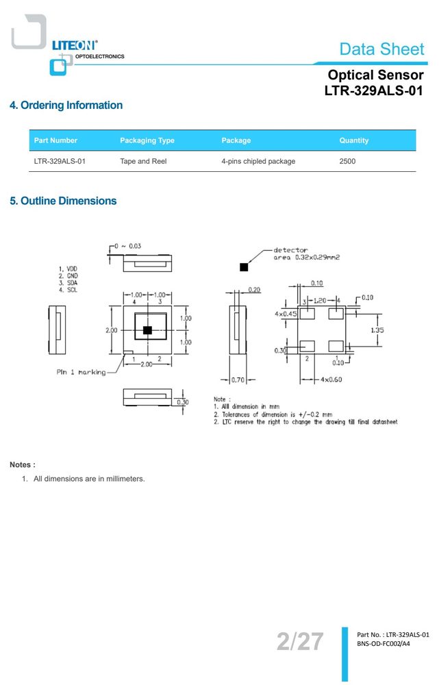
图纸取自原厂规格书,点击可放大查看原始尺寸标注。
引脚定义与内部结构
| 引脚 | 符号 | 名称 |
|---|---|---|
| 1 | VDD | |
| 2 | GND | |
| 3 | I/O | |
| 4 | I |
数据来源:原厂规格书引脚图
关键参数速览
- 电源电压 VCC
- 3.8
产品特点 Features
- I2C interface (Fast Mode @ 400kbit/s)
- Ultra-small ChipLED package
- Built-in temperature compensation circuit
- Low active power consumption with standby mode
- Supply voltage range from 2.4V to 3.6V capable of 1.7V logic voltage
- Operating temperature range from -30 C to +70 C
- RoHS and Halogen free compliant
- Light Sensor
- Optical Sensor
- LTR-329ALS-01
- 6. Functional Block Diagram
- 7. Application Circuit
- 3/27 Pa rt N o. : LTR- 329A LS-0 1
- BNS-OD-FC002/A4
绝对最大额定值 Absolute Maximum Ratings(TA = 25°C)
超过下表数值可能造成器件永久损坏,设计时请留余量。
| 参数 | 符号 | 额定值 | 单位 |
|---|---|---|---|
| Supply Voltage | VDD | 3.8 | V |
| Digital Voltage Range | SCL, SDA, INT | -0.5 to 3.8 | V |
| Digital Output Current | SCL, SDA, INT | -1 to 20 | mA |
| Storage Temperature | T | -40 to 100 | C |
数据来源:原厂规格书
电气特性 Electrical Characteristics(TA = 25°C)
| 参数 | 符号 | 最小 | 最大 | 单位 |
|---|---|---|---|---|
| All specifications are at VBus = 1.8V, T = | 25C, unless otherwise noted. | |||
| SCL clock frequency | f | 1 | 400 | kHz |
| t | 0.6 | us | ||
| Set-up time for a repeated START condition | t | 0.6 | us | |
| Set-up time for STOP condition | t | 0.6 | us | |
| Data hold time | t | 0.3 | 0.9 | us |
| Data setup time | t | 100 | ns | |
| Definition of timing for I2C bus | ||||
| 10/27 | Part No. | : LTR -32 9ALS -01 | ||
| BNS-OD-FC002/A4 |
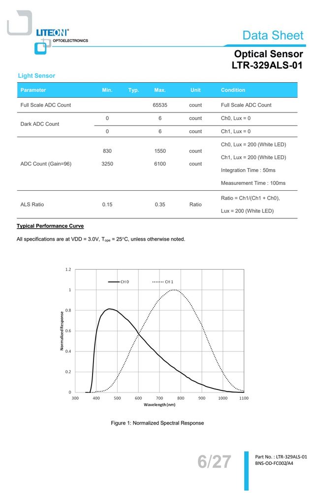
特性曲线(Typical Performance Curves)