
产品实拍图
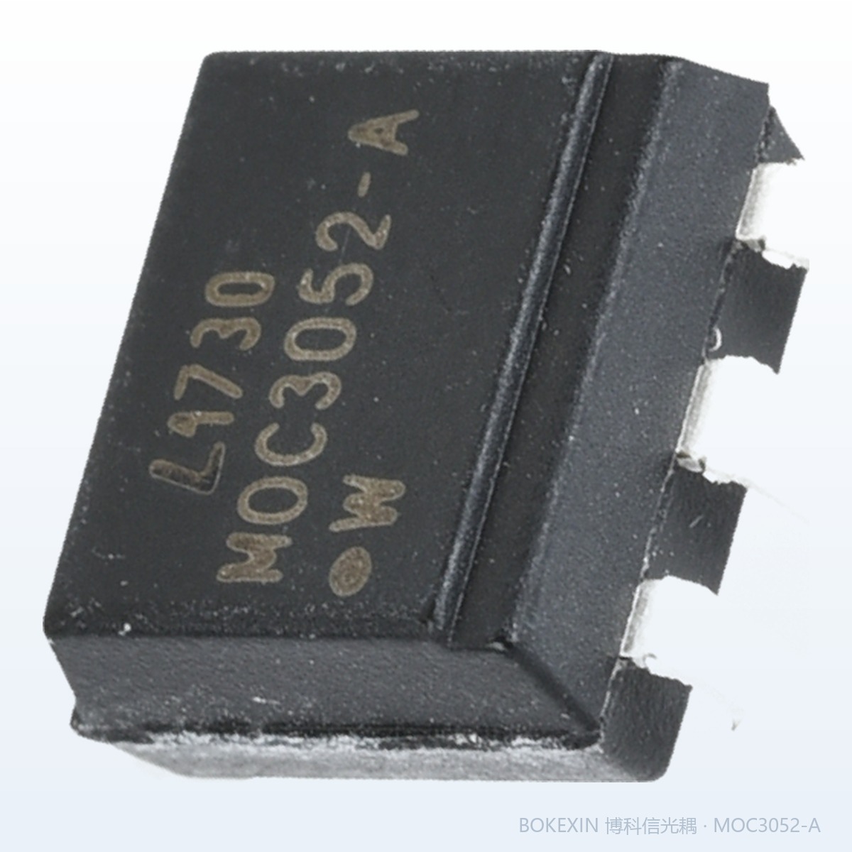
本页为博科信现货实拍(器件丝印 见规格书)。图片已加防盗水印,需要最新批次照片或未加水印原图请联系销售;点击图片可放大。
产品应用与封装尺寸
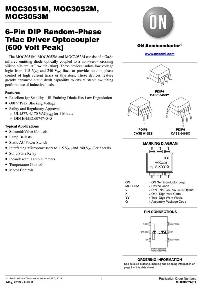
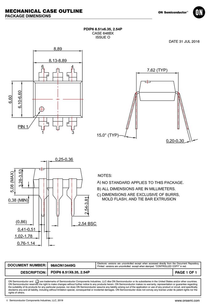
图纸取自原厂规格书,点击可放大查看原始尺寸标注。
关键参数速览
- 正向电压 VF
- 1.50
产品特点 Features
- greatly enhanced static dv/dt capability to ensure stable switching performance of inductive loads.
- PDIP6
- CASE 646BY
- Excellent I Stability—IR Emitting Diode Has Low Degradation
- 600 V Peak Blocking Voltage
- Temperature Minimum (Tsmin) 150°C
- Temperature Maximum (Tsmax) 200°C
- Time (t ) from (Tsmin to Tsmax) 60 seconds to 120 seconds
- Ramp−up Rate (T to T ) 3°C/second maximum
- Liquidous Temperature (T ) 217°C
- Time (t ) Maintained Above (T ) 60 seconds to 150 seconds
- Peak Body Package Temperature 260°C +0°C / –5°C
- Time (t ) within 5°C of 260°C 30 seconds
- Ramp−down Rate (T to T ) 6°C/second maximum
- Time 25°C to Peak Temperature 8 minutes maximum
- MOC3051M, MOC3052M, MOC3053M
安全与绝缘额定值(DIN EN/IEC 60747−5−5)
| 符号 | 参数 | 值 | 单位 |
|---|---|---|---|
| the safety ratings shall be ensured | by means of protective circuits. | ||
| Installation Classifications per DIN | VDE 0110/1.89 Table 1, < 150 V < 300 V | I–IV I–IV | |
| Pollution Degree (DIN VDE 0110/1.89) | 2 | ||
| Comparative Tracking Index | 175 | ||
| V Input−to−Output | Test Voltage, Method A, V x 1.6 = V , | Type and 1360 | Vpeak |
| Sample Test | with t = 10 s, Partial Discharge < 5 pC | ||
| Input−to−Output | Test Voltage, Method B, V x 1.875 = V | , 1594 | Vpeak |
| 100% Production | Test with t = 1 s, Partial Discharge < 5 pC | ||
| V Highest | Allowable Over−Voltage | 6000 | Vpeak |
| External | Creepage | ≥ 7 | mm |
| External | Clearance | ≥ 7 | mm |
| External | Clearance (for Option TV, 0.4” Lead Spacing) | ≥ 10 | mm |
| R Insulation | Resistance at T , V = 500 V | > 109 | kΩ |
| MOC3051M, MOC3052M, | MOC3053M | ||
| MAXIMUM RATINGS T = | 25°C unless otherwise specified. | ||
| T Storage Temperature | −40 to +150 | °C | |
| T Operating Temperature | −40 to +85 | °C | |
| T Junction Temperature | Range | −40 to +100 | °C |
| T Lead Solder | Temperature | 260 for 10 seconds | °C |
| P Total Device Power | Dissipation at 25°C Ambient | 330 | mW |
| Derate Above 25°C | 4.4 | mW/°C | |
| I Continuous Forward | Current | 60 | mA |
| P Total Power Dissipation | at 25°C Ambient | 100 | mW |
| Derate Above 25°C | 1.33 | mW/°C | |
| V Off−State Output | Terminal Voltage | 600 | V |
| I Peak Non−Repetitive | Surge Current (Single Cycle 60 Hz Sine Wave) | 1 | A |
| P Total Power Dissipation | at 25°C Ambient | 300 | mW |
| Derate Above 25°C | 4 | mW/°C | |
| should not be assumed, damage | may occur and reliability may be affected. |
电气特性 Electrical Characteristics(TA = 25°C)
| 符号 | 参数 | Characteristic | 最小 | 典型 | 最大 | 单位 |
|---|---|---|---|---|---|---|
| V Input | Forward Voltage | I = 10 mA | 1.18 | 1.50 | V | |
| I Peak | Blocking Current, Either Direction | V = 600 V, I = 0 | 10 | 100 | nA | |
| V Peak | On−State Voltage, Either Direction | I = 100 mA peak, | 2.2 | 2.5 | V | |
| dv/dt Critical | Rate of Rise of Off−State Voltage | I = 0, V = 600 V | 1000 | V/µs | ||
| I LED | Trigger Current, Main Terminal | MOC3051M MOC3052M MOC3053M | 15 10 6 | mA | ||
| I Holding | Current, | All | 540 | µA |
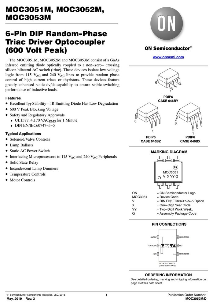
特性曲线(Typical Performance Curves)
订货信息与供货形式
| 器件 | 封装 | 包装 |
|---|---|---|
| MOC3051M | DIP 6−Pin | Tube (50 Units) |
| MOC3051SM | SMT 6−Pin (Lead Bend) | Tube (50 Units) |
| MOC3051VM | DIP 6−Pin, DIN EN/IEC60747−5−5 Option | Tube (50 Units) |
| MOC3051SVM | SMT 6−Pin (Lead Bend), | Tube (50 Units) |
| MOC3051TVM | DIP 6−Pin, 0.4” Lead Spacing, | Tube (50 Units) |