产品应用与封装尺寸
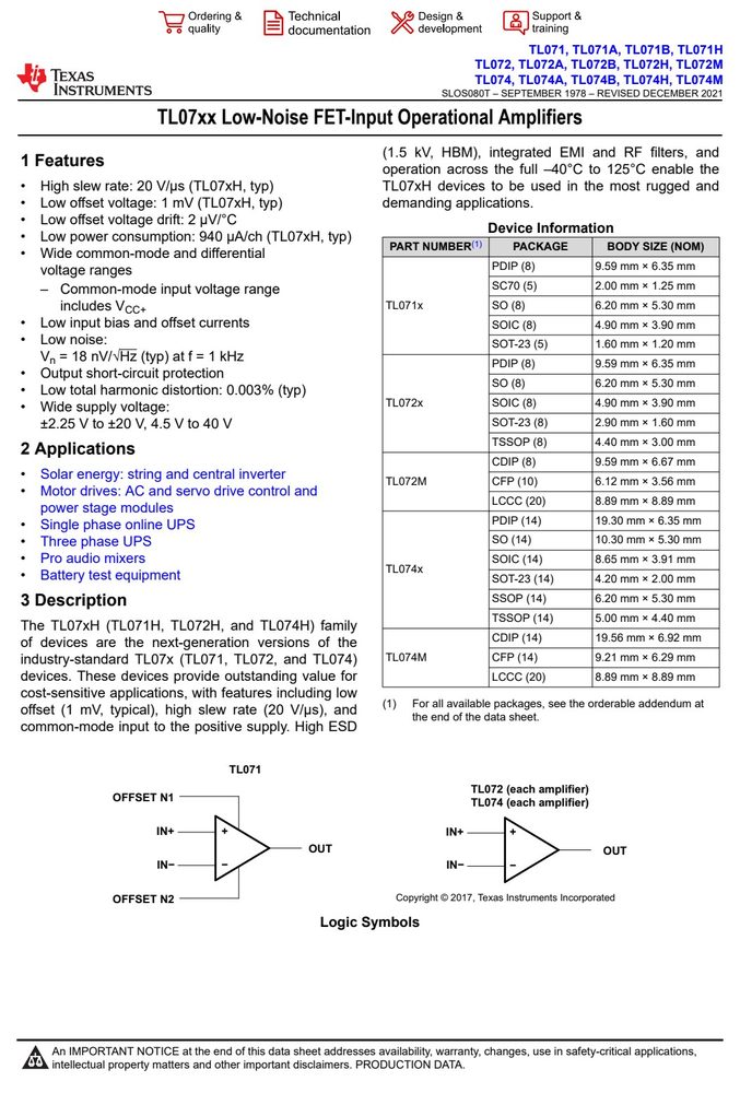
图纸取自原厂规格书,点击可放大查看原始尺寸标注。
引脚定义与内部结构
| 引脚 | 符号 | 名称 |
|---|---|---|
| 2 | I | |
| 3 | I | |
| 4 | V | |
| 5 | NC | |
| 6 | OUT |
数据来源:原厂规格书引脚图
关键参数速览
- 电源电压 VCC
- 42
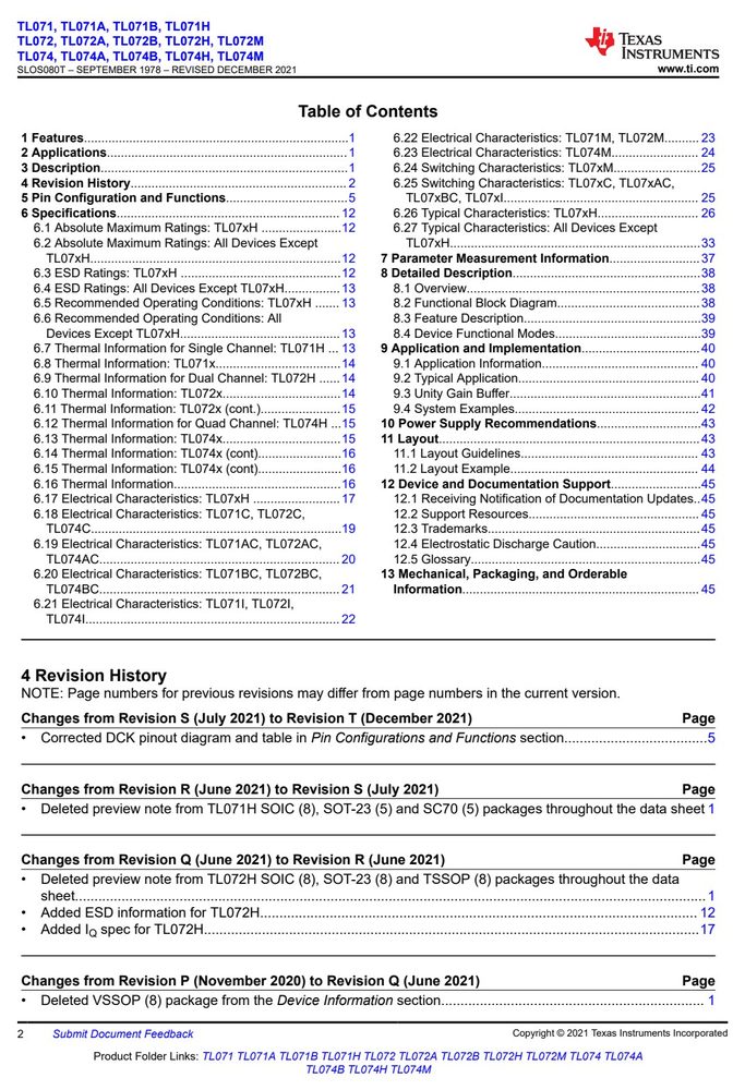
产品特点 Features
- operation across the full –40°C to 125°C enable the
- High slew rate: 20 V/μs (TL07xH, typ) TL07xH devices to be used in the most rugged and
- Low offset voltage: 1 mV (TL07xH, typ) demanding applications.
- Low offset voltage drift: 2 μV/°C
- Device Information
- Low power consumption: 940 μA/ch (TL07xH, typ)
- PART NUMBER(1) PACKAGE BODY SIZE (NOM)
- Wide common-mode and differential voltage ranges PDIP (8) 9.59 mm × 6.35 mm
- Common-mode input voltage range SC70 (5) 2.00 mm × 1.25 mm includes V TL071x SO (8) 6.20 mm × 5.30 mm
- Low input bias and offset currents
- SOIC (8) 4.90 mm × 3.90 mm
- Low noise:
- SOT-23 (5) 1.60 mm × 1.20 mm
- V = 18 nV/√Hz (typ) at f = 1 kHz n PDIP (8) 9.59 mm × 6.35 mm
- Output short-circuit protection
- SO (8) 6.20 mm × 5.30 mm
绝对最大额定值 Absolute Maximum Ratings(TA = 25°C)
超过下表数值可能造成器件永久损坏,设计时请留余量。
| 最小 | 最大 | 单位 |
|---|---|---|
| over operating ambient temperature range (unless otherwise noted) (1) | ||
| Supply voltage, V = (V ) – (V ) 0 | 42 | V |
| Common-mode voltage (3) (V ) – 0.5 | (V ) + 0.5 | V |
| Signal input pins Differential voltage (3) | V + 0.2 | V |
| Current (3) –10 | 10 | mA |
| Output short-circuit (2) Continuous | ||
| Operating ambient temperature, T –55 | 150 | °C |
| Junction temperature, T | 150 | °C |
| Storage temperature, T –65 | 150 | °C |
| (2) Short-circuit to ground, one amplifier per package. | ||
| over operating free-air temperature range (unless otherwise noted) (1) | ||
| V - V Supply voltage –0.3 | 36 | V |
| V Input voltage (3) V – 0.3 | V + 36 | V |
| I Input clamp current | –50 | mA |
| T Operating virtual junction temperature | 150 | °C |
| Case temperature for 60 seconds - FK package | 260 | °C |
| Lead temperature 1.8 mm (1/16 inch) from case for 10 seconds | 300 | °C |
| T Storage temperature –65 | 150 | °C |
| TL071, | TL071A, TL071B, | TL071H |
| TL072, TL072A, | TL072B, TL072H, | TL072M |
| TL074, TL074A, | TL074B, TL074H, | TL074M |
数据来源:原厂规格书
电气特性 Electrical Characteristics(TA = 25°C)
| 参数 | 测试条件 | 最小 | 典型 | 最大 | 单位 |
|---|---|---|---|---|---|
| S CC+ CC– | A | L | S ±1 | CM S ±4 | |
| V Input offset voltage | mV | ||||
| T = –40°C to 125°C | ±5 | ||||
| dV /dT Input offset voltage drift | T = –40°C to 125°C | ±2 | µV/℃ | ||
| PSRR | S CM S T = –40°C to 125°C | ±1 | ±10 | μV/V | |
| Channel separation f | = 0 Hz | 10 | µV/V | ||
| ±1 | ±120 | pA | |||
| T = –40°C to 125°C | (1) | ±5 | nA | ||
| ±0.5 | ±120 | pA | |||
| T = –40°C to 125°C | (1) | ±5 | nA | ||
| f | = 1 kHz | 37 | |||
| e Input voltage noise density | nV/√Hz | ||||
| f | = 10 kHz | 21 | |||
| i Input current noise f | = 1 kHz | 80 | fA/√Hz | ||
| V | (V ) + 1.5 | (V ) | V | ||
| CM range | CC– | CC+ | |||
| CMRR | 100 | 105 | dB | ||
| CMRR | T = –40°C to 125°C | 95 | dB | ||
| CMRR | 90 | 105 | dB | ||
| CMRR | T = –40°C to 125°C | 80 | dB | ||
| Z Differential | 100 || 2 | MΩ || pF | |||
| Z Common-mode | 6 || 1 | TΩ || pF | |||
| A Open-loop voltage gain | (V ) + 0.3 V < V < (V ) T = –40°C to 125°C | 118 | 125 | dB | |
| A Open-loop voltage gain | 2 kΩ, (V ) + 1.2 V < V < T = –40°C to 125°C | 115 | 120 | dB | |
| GBW Gain-bandwidth product | 5.25 | MHz | |||
| SR Slew rate | V = 40 V, G = +1, C = 20 pF | 20 | V/μs | ||
| To 0.1%, V = 40 V, V = 10 V , G = +1, CL = 20 | pF | 0.63 | |||
| To 0.1%, V = 40 V, V = 2 V , G = +1, CL = 20 pF | 0.56 | ||||
| t Settling time | μs | ||||
| To 0.01%, V = 40 V, V = 10 V , G = +1, CL = 20 | pF | 0.91 | |||
| To 0.01%, V = 40 V, V = 2 V , G = +1, CL = 20 | pF | 0.48 | |||
| Phase margin | G = +1, R = 10kΩ, C = 20 pF | 56 | ° | ||
| Overload recovery time | V × gain > V | 300 | ns | ||
| Product Folder Links: | TL071 TL071A TL071B TL071H TL072 TL072A | TL072B TL072H TL072M | TL074 | TL074A | |
| S CC+ CC– | A | L | S | CM S | |
| THD+N | V = 40 V, V = 6 V , G = +1, f = 1 kHz | 0.00012 | % | ||
| EMIRR EMI rejection ratio f | = 1 GHz | 53 | dB | ||
| V = 40 V, R = 10 kΩ | 115 | 210 | |||
| Voltage output swing from | V S = 40 V, R L = 2 kΩ | 520 | 965 | ||
| rail | V = 40 V, R = 10 kΩ | 105 | 215 | ||
| V = 40 V, R = 2 kΩ | 500 | 1030 | |||
| I Short-circuit current | ±26 | mA | |||
| C Capacitive load drive | 300 | pF | |||
| Z f | = 1 MHz, I = 0 A | 125 | Ω | ||
| I | = 0 A | 937.5 | 1125 | ||
| I | = 0 A, (TL071H) | 960 | 1156 | ||
| I I | = 0 A | 1130 | µA | ||
| I | = 0 A, (TL072H) T = –40°C to 125°C | 1143 | |||
| I | = 0 A, (TL071H) | 1160 | |||
| Turn-On Time | At T = 25°C, V = 40 V, V ramp rate > 0.3 V/µs | 60 | μs | ||
| Product Folder Links: | TL071 TL071A TL071B TL071H TL072 TL072A | TL072B TL072H TL072M | TL074 | TL074A | |
| TL071, | TL071A, | TL071B, | TL071H | ||
| TL072, TL072A, | TL072B, | TL072H, | TL072M | ||
| TL074, TL074A, | TL074B, | TL074H, | TL074M |
特性曲线(Typical Performance Curves)