
产品应用与封装尺寸
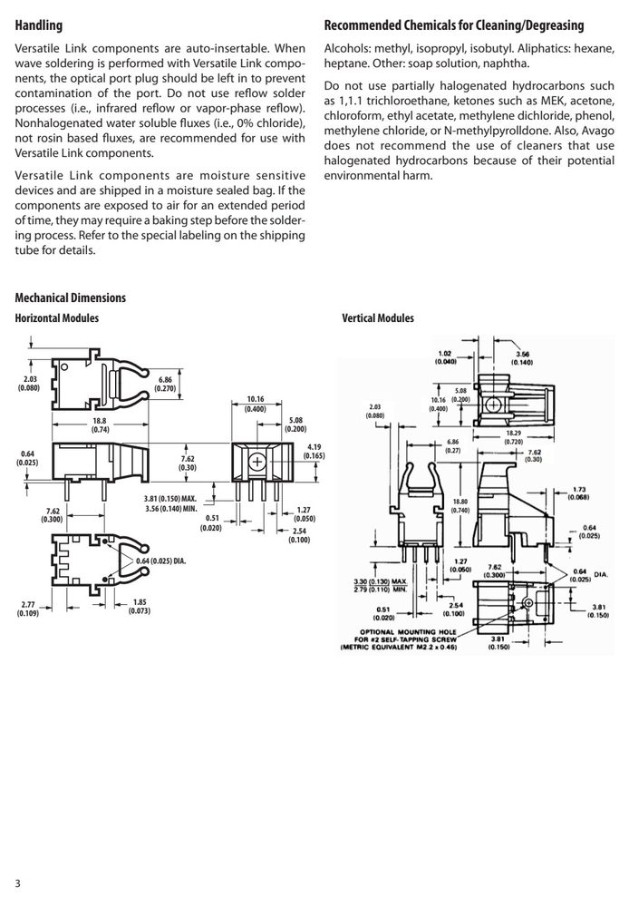
图纸取自原厂规格书,点击可放大查看原始尺寸标注。
关键参数速览
- 正向电压 VF
- 1.67 2.02
- 电源电压 VCC
- 3
- 工作温度 TA
- +85
产品特点 Features
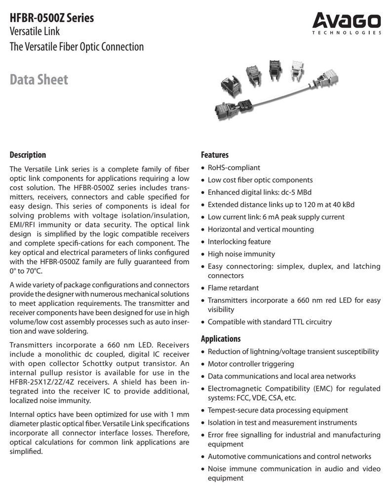
- The Versatile Link series is a complete family of fiber
- RoHS-compliant and complete specifi-cations for each component. The
- HFBR-0500Z Series Part Number Guide
- HFBR X5XXZ
- 1 = Transmitter
- 2 = Receiver Z = RoHS-compliant
- 5 = 600 nm Transmitter and
- Receiver Products 1 = 5 MBd High Performance Link
- 2 = 1 MBd High Performance Link
- 3 = 40 kBd Low Current/Extended Distance Link
- 2 = Horizontal Package 4 = 1 MBd Standard Link
- 3 = Vertical Package 6 = 155 MBd Receiver
- 7 = 155 MBd Transmitter
- 8 = 10 MBd High Performance Link
- Link Selection Guide
- (Links specified from 0 to 70°C, for plastic optical fiber unless specified.)
绝对最大额定值 Absolute Maximum Ratings(TA = 25°C)
超过下表数值可能造成器件永久损坏,设计时请留余量。
| 参数 | 符号 | 最小 | 最大 | 单位 | Reference |
|---|---|---|---|---|---|
| Storage Temperature | T | –40 | +85 | °C | |
| Operating Temperature | T | –40 | +85 | °C | |
| Lead Soldering Cycle | Temp. | 260 | °C | Note 1, 4 | |
| Time | 10 | sec | |||
| Forward Input Current | I I | 1000 80 | mA | Note 2, 3 | |
| Storage Temperature | T | –40 | +85 | °C | |
| Operating Temperature | T | –40 | +85 | °C | |
| Lead Soldering Cycle | Temp. | 260 | °C | Note 1, 4 | |
| Time | 10 | sec | |||
| Forward Input Current | I I | 1000 80 | mA | Note 2, 3 | |
| Transmitter Electrical/Optical | Characteristics 0°C to 70°C unless | otherwise specified. | |||
| Transmitter HFBR-15X2Z | P –13.6 | –4.5 | dBm I | = 60 mA | |
| Output | –11.2 | –5.1 | I | = 60 mA, 25°C | |
| Optical HFBR-15X4Z | P –17.8 | –4.5 | dBm I | = 60 mA | |
| Power | –15.5 | –5.1 | I | = 60 mA, 25°C | |
| Output Optical Power | ∆P /∆T | –0.85 | %/°C | ||
| Peak Emission Wavelength | λPK | 660 | nm | ||
| Forward Voltage | V 1.45 | 1.67 2.02 | V I | = 60 mA | |
| Forward Voltage | ∆V /∆T | –1.37 | mV/°C | Fig. 11 | |
| Effective Diameter | D | 1 | mm | ||
| Numerical Aperture | NA | 0.5 | |||
| Voltage | T | = 25°C | |||
| Diode Capacitance | C | 86 | pF V | = 0, f = 1 MHz | |
| Rise Time | t | 80 | ns 10% | to 90%, | Note 1 |
| Fall Time | t | 40 | ns I | = 60 mA | |
| HFBR-25X2Z/25X4Z Receivers | Pin # 1 | Function V | |||
| DO NOT CONNECT 5 | 2 | Ground | |||
| 1000 | 4 RL | 3 | V CC | ||
| 3 VCC | 4 | R L | |||
| GROUND | 5 | Do not | connect | ||
| VO | 8 | Do not | connect | ||
| electrically connect | these pins. | ||||
| Storage Temperature | T | –40 | +85 | °C | |
| Operating Temperature | T | –40 | +85 | °C | |
| Lead Soldering Cycle | Temp. | 260 | °C | Note 1, 3 | |
| Time | 10 | sec | |||
| Supply Voltage | V | –0.5 | 7 | V | Note 2 |
| Output Collector Current | I | 25 | mA | ||
| Output Collector Power Dissipation | P | 40 | mW | ||
| Output Voltage | V | –0.5 | 18 | V | |
| Pull-up Voltage | V | –5 | V | V | |
| Fan Out (TTL) | N | 5 | |||
| Receiver HFBR-2522Z | P –24 | dBm V = | 0 V | Notes 1, 2, 3 | |
| Optical Input | I = | 8 mA | |||
| Power Level HFBR-2524Z | –20 | Note 4 | |||
| Optical Input Power | P | -43 | dBm V = | 5.25 V | |
| Level Logic 1 | I = | ≤250 µA | |||
| High Level Output Current | I 5 | 250 | µA V = | 18 V, P = 0 | Note 5 |
| OH | O | R | |||
| Low Level Output Voltage | V 0.4 | 0.5 | V I = | 8 mA | Note 5 |
| High Level Supply Current | I 3.5 | 6.3 | mA V = P = | 5.25 V, 0 | Note 5 |
| Low Level Supply Current | I 6.2 | 10 | mA V = P = | 5.25 V, -12.5 dBm | Note 5 |
| Effective Diameter | D 1 | mm | |||
| Internal Pull-up Resistor | R 680 1000 | 1700 | Ω | ||
| F | PLH | PLH | |||
| Storage Temperature | T | –40 | +85 | °C | |
| Operating Temperature | T | –40 | +85 | °C | |
| Lead Soldering Cycle | Temp. | 260 | °C | Note 1, 4 | |
| Time | 10 | sec | |||
| Forward Input Current | I I | 1000 80 | mA | Note 2, 3 | |
| Transmitter Electrical/Optical | Characteristics 0°C to 70°C unless | otherwise | specified. | ||
| Transmitter Output | P –11.2 | –5.1 | dBm I | = 60 mA, 25°C | Notes 3, 4 |
| Optical Power | –13.6 | –4.5 | I | = 60 mA | |
| –35.5 | I | = 2 mA, 0-70°C | Fig. 9, 10 | ||
| Output Optical Power | ∆P /∆T –0.85 | %/°C | |||
| Peak Emission | λPK 660 | nm | |||
| Forward Voltage | V 1.45 1.67 | 2.02 | V I | = 60 mA | |
| Forward Voltage | ∆V /∆T –1.37 | mV/°C | Fig. 18 | ||
| Effective Diameter | D 1 | mm | |||
| Voltage | T = | 25°C | |||
| Diode Capacitance | C 86 | pF V = | 0, f = 1 MHz | ||
| Rise Time | t 80 | ns 10% | to 90%, | Note 1 | |
| Fall Time | t 40 | I = | 60 mA | ||
| Pin # 1 | Function V | ||||
| DO NOT CONNECT 5 | 2 | Ground | |||
| VCC | 3 | Open | |||
| 3 OPEN | 4 | V CC | |||
| GROUND | 5 | Do not | connect | ||
| VO | 8 | Do not | connect | ||
| Do not electrically | connect these | pins. | |||
| Storage Temperature | T | –40 | +85 | °C | |
| Operating Temperature | T | –40 | +85 | °C | |
| Lead Soldering Cycle | Temp. | 260 | °C | Note 1, 3 | |
| Time | 10 | sec | |||
| Supply Voltage | V | –0.5 | 7 | V | Note 2 |
| Average Output Collector Current | I | –1 | 5 | mA | |
| Output Collector Power Dissipation | P | 25 | mW | ||
| Output Voltage | V | –0.5 | 7 | V | |
| Input Optical Power | P –39 | –13.7 dBm | V = V , | I = 3.2 mA | Notes 1, |
| R(L) | O OL | OL | |||
| Level Logic 0 | –39 | –13.3 | V = V | , | 2, 3 |
| I = 8 | mA, 25°C | ||||
| Input Optical Power | P | –53 dBm | V = 5.5 | V | Note 3 |
| Level Logic 1 | I = ≤40 | µA | |||
| High Level Output Voltage | V 2.4 | V | I = -40 | µA, P = 0 µW | |
| OH | O | R |
数据来源:原厂规格书